Two-dimensional silylene film and preparation method thereof

A silicene and thin film technology, applied in the field of two-dimensional silicene thin film and its preparation, can solve the problems of lack of silicene preparation technology, hindering experimental research progress, lack of silicene preparation technology and characterization technology, etc. simple effect

Active Publication Date: 2014-03-26
ZHEJIANG UNIV
View PDF6 Cites 15 Cited by
  • Summary
  • Abstract
  • Description
  • Claims
  • Application Information

AI Technical Summary

Problems solved by technology

[0007] Affected by graphene, although there are many theoretical studies on silicene, due to the lack of preparation technology and characterization technology of silicene, the purposeful experimental research on silicene is still very limited (or when growing silicon nanowires, at the same time There are

Method used


Image

  • Two-dimensional silylene film and preparation method thereof
  • Two-dimensional silylene film and preparation method thereof
  • Two-dimensional silylene film and preparation method thereof

Examples


Embodiment 1

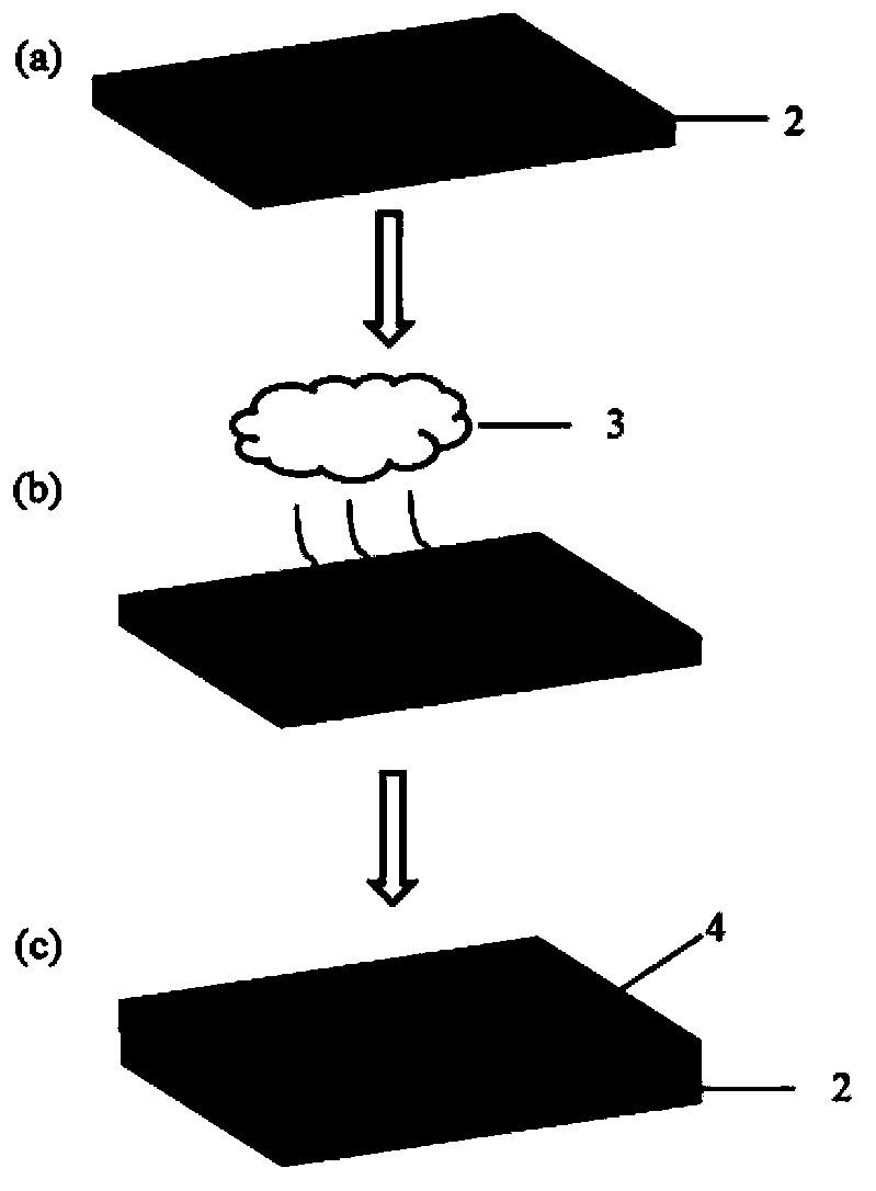
[0039] like figure 1 shown in 1×10 -9 Under the ultra-high vacuum of Pa, heat-treat the SiC catalytic layer with a thickness of 25mm at 1600°C for 10 minutes; then pass it into Ar:H 2 : SiHCl 3 (100sccm: 10sccm: 5sccm), the silicene film was prepared by ultra-high vacuum chemical vapor deposition for 5 minutes; finally, the temperature was lowered to 20°C at a cooling rate of 400°C / min, so that two layers were grown on SiC silicene thin films4.

[0040] In this example, SiC is both the substrate 1 and the catalytic layer 2, SiHCl 3 As the gaseous silicon source 3, a 2-layer silicene film 4 was synthesized.

Embodiment 2

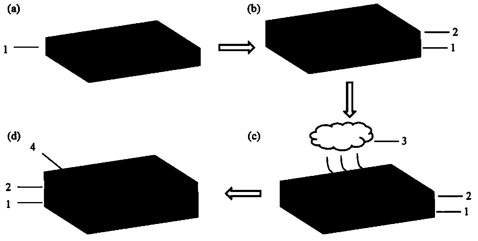
[0042] like figure 1 As shown, for Al with a thickness of 10mm 2 o 3 Plasma treatment was carried out for 5 minutes, and SiH was injected at 240°C by plasma-enhanced CVD 4 (20sccm) and water vapor (10sccm) for 20 minutes to prepare a silicene film, and then lower the temperature to 20°C at a cooling rate of 0.2°C / min to obtain a silicene film 4 with 10 layers.

[0043] In this example, Al with a thickness of 10mm 2 o 3 Both substrate 1 and catalyst layer 2, SiH 4 is the silicon source 3.

Embodiment 3

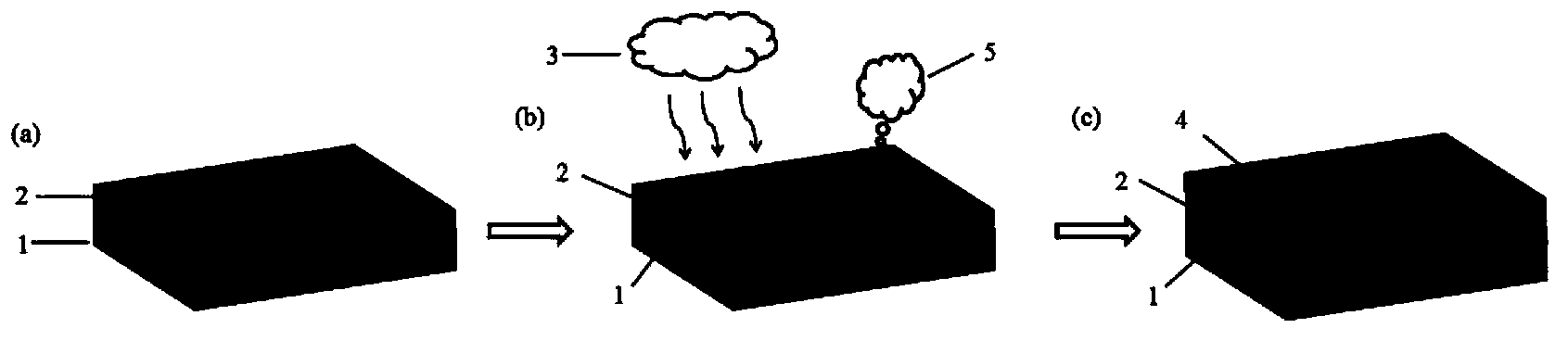
[0045] like figure 1 As shown, MgO with a thickness of 2 mm was heat-treated at 600 °C for 20 minutes; then, silicene films were prepared at 300 °C by microwave plasma-enhanced CVD: for liquid Si 3 h 8 The silicon source 3 is heated to generate steam, and the generated steam (20 sccm) and Ar (100 sccm) are passed into the silicene film synthesis chamber, the temperature of the catalytic layer is 300 ° C, and the Si is stopped after 20 minutes of growth. 3 h 8 Steam and Ar; modified N 2 And the temperature is lowered to 20° C. at a cooling rate of 80° C. / min, thereby obtaining a silicene thin film 4 with an uneven number of layers (40-50 layers).

[0046] In this example, MgO is both substrate 1 and catalyst layer 2, liquid Si 3 h 6 The steam generated is the silicon source 3 .


PUM

PropertyMeasurementUnit
Thicknessaaaaaaaaaa

Abstract

The invention discloses a method for growing a two-dimensional silylene film from a gaseous silicon source. According to the method, the silylene film is prepared through releasing silicon atom groups on a catalytic layer from the gaseous silicon source by adopting a chemical vapor deposition or physical vapor deposition technology, wherein the thickness of the catalytic layer is 25nm to 25mm, and the temperature of the catalytic layer is controlled to be 20-1,600 DEG C. The method disclosed by the invention is simple and easy to implement. The prepared silylene film is a two-dimensional layered film which is formed in a manner that three, four, five or seven silicon atoms serve as repeating units and are connected by covalent bonds, and the number of contained silylene layers is 1-200.

Description

technical field [0001] The invention relates to a two-dimensional silicene film and a preparation method thereof, in particular to a method for growing a silicene film on a catalytic layer by using a gaseous silicon source. Background technique [0002] Nanomaterials include zero-dimensional, one-dimensional and two-dimensional materials. Nanomaterials have different photoelectric, chemical, thermal and other properties from bulk materials; The research and development of materials is a matter of recent years, especially the research on graphene since 2004. Two-dimensional nanomaterials mainly include layered films composed of elements in the fourth main group of the periodic table, such as graphene (composed of carbon elements), silicene (composed of silicon elements), germanene (composed of germanium elements), metal sulfur family compounds such as MoS 2 , W 2 And GaS, etc., and layered materials such as boron nitride. At present, the most researched two-dimensional na...

Claims


Application Information

Patent Timeline
IPC IPC(8): C30B29/06C30B29/64C30B23/00C30B25/00C23C14/14C23C16/24
Inventor 徐明生陈红征
Owner ZHEJIANG UNIV
Why Eureka
Try Eureka