Solar cell panel, manufacturing method thereof and solar cell comprising solar cell panel

A solar cell panel and silicon nitride layer technology, applied in the field of solar cells, can solve the problems of solar cell light-induced attenuation and achieve the effects of suppressing light-induced attenuation, high photoelectric conversion efficiency, and reducing light-induced attenuation

Active Publication Date: 2014-03-05
YINGLI ENERGY CHINA
View PDF6 Cites 0 Cited by
  • Summary
  • Abstract
  • Description
  • Claims
  • Application Information

AI Technical Summary

Problems solved by technology

[0009] The present invention aims to provide a solar cell panel, its preparation method and a solar cell comprising it, so as to solve the problem of serious light-induced attenuation of solar cells in the prior art

Method used


Image

  • Solar cell panel, manufacturing method thereof and solar cell comprising solar cell panel
  • Solar cell panel, manufacturing method thereof and solar cell comprising solar cell panel
  • Solar cell panel, manufacturing method thereof and solar cell comprising solar cell panel

Examples


preparation example Construction

[0032] In addition, the present invention also provides a method for preparing a solar cell panel, which includes the step of disposing a silicon nitride film on the surface of the silicon wafer, wherein the step of disposing the silicon nitride film on the surface of the silicon wafer includes: disposing a second silicon nitride film on the silicon wafer A silicon nitride layer; a second silicon nitride layer with a higher refractive index than the first silicon nitride layer is set on the first silicon nitride layer.

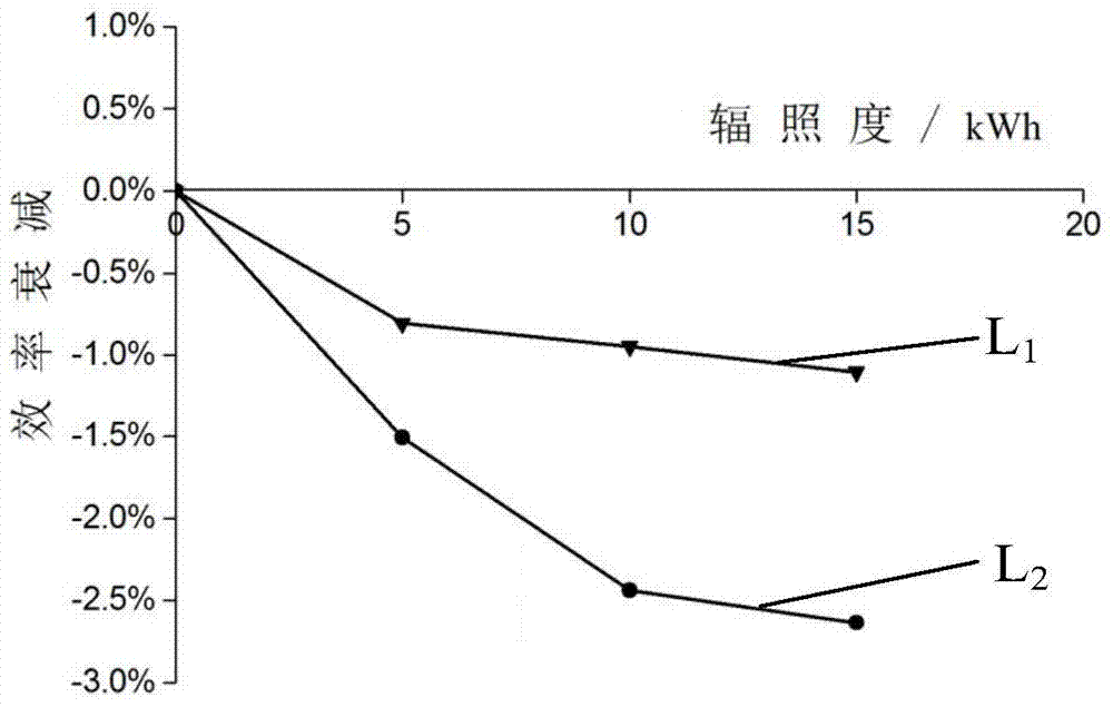
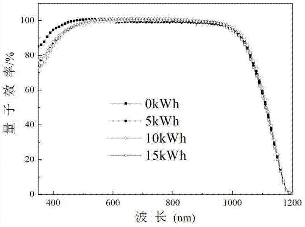
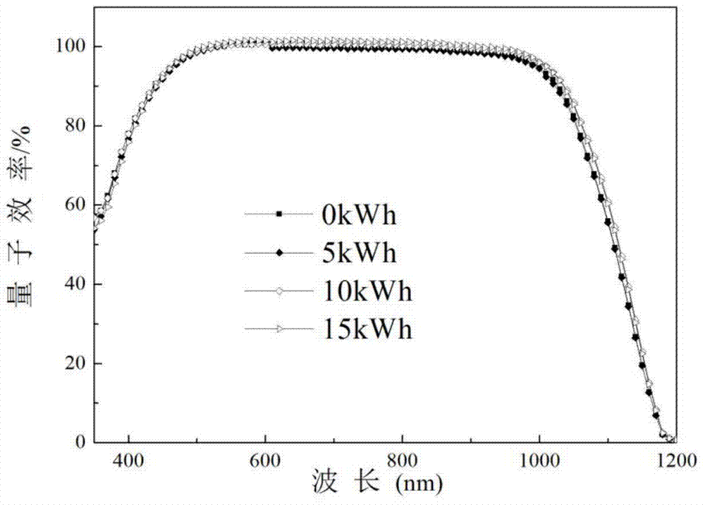
[0033]In the solar panel formed by the above method, since the silicon nitride layer on the outer layer of the silicon wafer has a higher refractive index, the surface of the silicon wafer has a stronger blocking effect on ultraviolet rays, thereby effectively weakening the intensity of ultraviolet rays entering the silicon nitride film. This can prevent the incoming ultraviolet light from activating the K inside the silicon nitride film to a certain extent. 0...

Embodiment 1

[0042] A silicon nitride film is deposited on the surface of the silicon wafer by PECVD. The specific process flow is as follows: the deposition temperature is set to 300°C, the conveyance speed of the boat is 205cm / min, and the gas flow in the six groups of intake pipes is set to the following flow:

[0043]

[0044] Through the above process flow, a silicon wafer provided with a silicon nitride film is obtained, and a solar battery panel is prepared from the silicon wafer.

Embodiment 2

[0046] A silicon nitride film is deposited on the surface of the silicon wafer by PECVD. The specific process flow is as follows: the deposition temperature is set to 300°C, the conveyance speed of the boat is 205cm / min, and the gas flow in the six groups of intake pipes is set to the following flow:

[0047]

[0048] Through the above process flow, a silicon wafer provided with a silicon nitride film is obtained, and a solar battery panel is prepared from the silicon wafer.


PUM

PropertyMeasurementUnit
Thicknessaaaaaaaaaa
Thicknessaaaaaaaaaa

Abstract

The invention discloses a solar cell panel, a manufacturing method of the solar cell panel and a solar cell comprising the solar cell panel. The solar cell panel comprises a silicon wafer and a silicon nitride film arranged on the silicon wafer, wherein the silicon nitride film comprises a first silicon nitride layer and a second silicon nitride layer, the first silicon nitride layer is formed on the silicon wafer, the second silicon nitride layer is formed on the first silicon nitride layer, and the refractive index of the second silicon nitride layer is larger than that of the first silicon nitride layer. The surface of the silicon wafer in the solar cell panel is provided with the silicon nitride film of a two-layer structure, and the refractive index of the second silicon nitride layer arranged on the outer side is made to be larger than that of the first silicon nitride layer. The ultraviolet light blocking function of the surface of the silicon nitride film can be enhanced, and then the intensity of ultraviolet light entering the silicon nitride film is reduced. The ultraviolet light entering can be stopped from activating K0 groups in the silicon nitride film to a certain degree, and then generation of electric charge trapping centers is reduced, so that the light degradation problem of the solar cell is solved.

Description

technical field [0001] The invention relates to the field of solar cell manufacturing, in particular to a solar cell panel, a preparation method thereof and a solar cell comprising the same. Background technique [0002] With the increasingly serious problem of energy shortage, the development and application of solar cells are getting more and more attention. The manufacture of solar cells is mostly based on silicon materials, which are formed by doping boron elements in the materials to form N-type semiconductors, and further form silicon wafers for solar cell panels. During the preparation of silicon materials, since the quartz crucible used for heating the silicon liquid contains oxygen impurities, these oxygen impurities will inevitably be brought into the silicon material, and then into the silicon wafer. [0003] When the solar cell is in a light environment, the oxygen impurities in the silicon wafer are easy to recombine with boron and impurity iron to form B-O and...

Claims


Application Information

Patent Timeline
IPC IPC(8): H01L31/0216H01L31/18
CPCH01L31/02165H01L31/02167Y02E10/50Y02P70/50
Inventor 马继奎徐卓李永超孙宁宁安海娇
Owner YINGLI ENERGY CHINA
Why Eureka
Try Eureka