A process of manufacturing printed antenna by using pin feed point
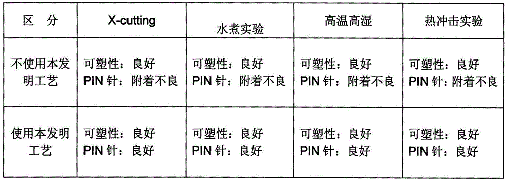
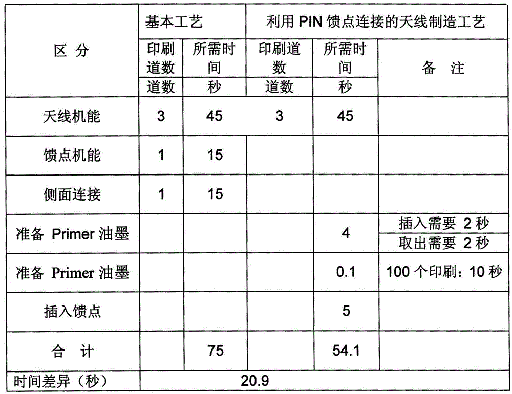
A printing antenna and process technology, applied in the direction of antenna support/installation device, radiating element structure, etc., can solve the problems of weak bonding, drop, short circuit, etc. between the antenna and the metal or plastic frame, and shorten the printing time , Improve productivity, and reduce time
- Summary
- Abstract
- Description
- Claims
- Application Information
AI Technical Summary
Problems solved by technology
Method used
Image

Examples
Embodiment 1
[0027] A process for manufacturing a printed antenna utilizing a PIN feed point, the process includes the following steps:
[0028] (1) Use screen printing to print ink with strong adhesion on the PIN pin, and the PIN pin is made of copper material;
[0029] (2) drying at 60°C;
[0030] (3) The PIN pin that step (2) gained is printed with ink adopts conventional hot-melt technology to heat-melt onto the plastic casing of the antenna to be printed;
[0031] (4) Use conductive ink to print the antenna on the frame or casing by screen printing;
[0032] (5) drying at 80°C to obtain the product.
[0033] The strong printing ink (being Primer printing ink) of the adhesive strength that adopts in the above-mentioned steps comprises the component of following weight portion content: basic resin acrylic resin (Acrylresin) 30; Auxiliary resin isocyanate resin (Isocyanateresin) 5; Adhesive agent 0.5; Thickener 0.5; organic solvent benzene 21. The above-mentioned inks can be prepared...
Embodiment 2
[0040] A process for manufacturing a printed antenna utilizing a PIN feed point, the process includes the following steps:
[0041] (1) On the PIN needle, the ink with strong adhesion is printed by transfer printing, and the material of the PIN needle is a gold-plated plastic PIN needle;
[0042](2) drying at 120°C;
[0043] (3) Insert the PIN pin printed with ink obtained in step (2) into the frame or casing of the antenna to be printed using conventional ultrasonic technology;
[0044] (4) Use conductive ink to print the antenna on the frame by transfer printing;
[0045] (5) drying at 120°C to obtain the product.
[0046] The strong printing ink (being Primer printing ink) that adopts in the above-mentioned steps comprises the component of following weight portion content: basic resin acrylic resin (Acrylresin) 50; Auxiliary resin isocyanate resin (Isocyanateresin) 15; Adhesive agent 2.0; Thickener 2.0; organic solvent xylene 21. The above-mentioned inks can be prepared...
Embodiment 3
[0049] A process for manufacturing a printed antenna utilizing a PIN feed point, the process includes the following steps:
[0050] (1) Print ink with strong adhesion on the PIN needle by pad printing, and the material of the PIN needle is silver-plated plastic PIN needle;
[0051] (2) drying at 100°C;
[0052] (3) Insert the PIN pin printed with ink obtained in step (2) into the frame or casing of the antenna to be printed using conventional cold pressing technology;
[0053] (4) Use conductive ink to print the antenna on the frame by transfer printing;
[0054] (5) drying at 100°C to obtain the product.
[0055] The strong printing ink (being Primer printing ink) that adopts in the above-mentioned steps comprises the component of following weight portion content: basic resin alkyd resin (Alkydresin) 35; Auxiliary resin amino resin (Aminoresin) 8; Adhesive agent 1; Thickening Agent 1; organic solvent acetic acid 30. The above-mentioned inks can be prepared by conventional...
PUM
 Abstract
Description
Claims
Application Information
 - R&D
- Intellectual Property
- Life Sciences
- Materials
- Tech Scout
- Unparalleled Data Quality
- Higher Quality Content
- 60% Fewer Hallucinations
Browse by: Latest US Patents, China's latest patents, Technical Efficacy Thesaurus, Application Domain, Technology Topic, Popular Technical Reports.
© 2025 PatSnap. All rights reserved.Legal|Privacy policy|Modern Slavery Act Transparency Statement|Sitemap|About US| Contact US: help@patsnap.com