Method and system for testing power semiconductor module packaging process

A technology of power semiconductors and testing methods, applied in the direction of semiconductor/solid-state device testing/measurement, semiconductor devices, electric solid-state devices, etc., can solve the problems of expensive equipment and unrepresentative X-ray detection technology

Inactive Publication Date: 2016-08-24
INST OF ELECTRICAL ENG CHINESE ACAD OF SCI
View PDF9 Cites 0 Cited by
  • Summary
  • Abstract
  • Description
  • Claims
  • Application Information

AI Technical Summary

Problems solved by technology

[0005] Usually, X-ray inspection technology requires very expensive equipment, and it also detects the quality of the process from a static point of view, which does not represent the actual situation of such a welding process and aluminum wire bonding under working conditions

Method used


Image

  • Method and system for testing power semiconductor module packaging process
  • Method and system for testing power semiconductor module packaging process
  • Method and system for testing power semiconductor module packaging process

Examples


Embodiment Construction

[0054] The present invention will be described in detail below with reference to the accompanying drawings and specific embodiments.

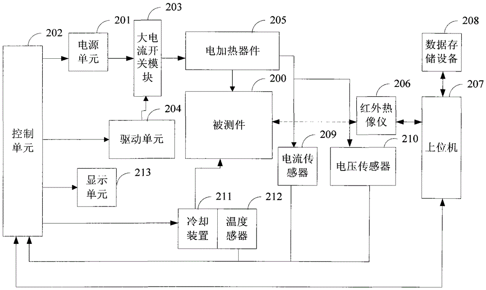
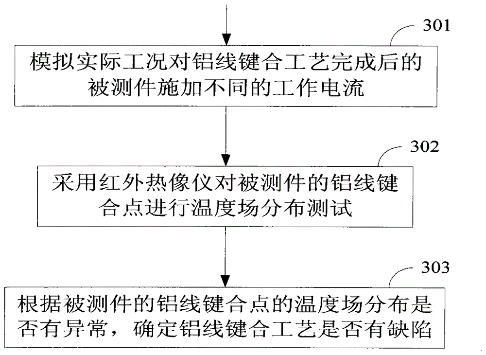
[0055] The present invention provides a test method and system for power semiconductor module chip welding process, a test method and system for power semiconductor module aluminum wire bonding process, and a packaging process including chip welding process and aluminum wire bonding process test The test method and system are used to realize the test of the chip bonding process and / or the aluminum wire bonding process under actual working conditions.

[0056] Examples are given below for description.

[0057] First, the test method of the power semiconductor module chip welding process of the present invention will be described.

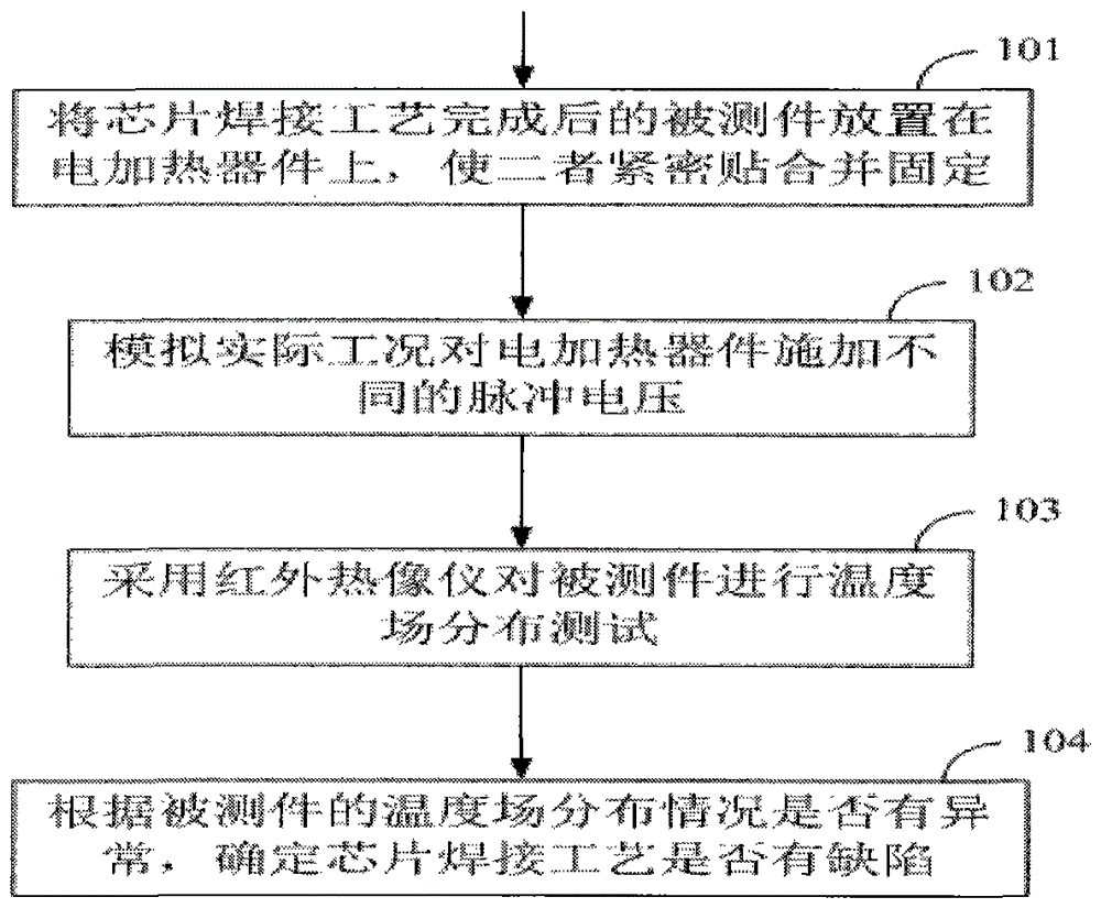
[0058] Such as figure 1 As shown, a preferred embodiment of the test method of the power semiconductor module chip welding process of the present invention comprises the following steps:

[0059] Step 101 , placing...


PUM


Abstract

The invention discloses a method and system for testing the power semiconductor module chip welding technology, a method and system for testing the power semiconductor module aluminum wire bonding technology, and a method and system for testing the packaging technology comprising the chip welding technology and the aluminum wire bonding technology. According to the method and system, an electric heating device is used for simulating working conditions, the impulse voltage / current is applied to the electric heating device, and / or the loop testing voltage / current is applied to heat a tested piece after chip welding, or the working voltage / current and / or the loop testing voltage / current are / is applied to a tested piece after aluminum wire bonding, and a heat infrared imager is adopted to conduct temperature field distribution testing on the tested piece. Whether the chip welding technology and / or the aluminum wire bonding technology have / has defects or not is determined according to the fact whether the temperature field distribution condition of the tested piece or an aluminum wire bonding point of the tested piece is abnormal or not. Dynamic monitoring on the chip welding technology and / or the aluminum wire bonding technology under actual working conditions is achieved, and the testing cost is reduced.

Description

technical field [0001] The invention relates to semiconductor testing technology, in particular to a testing method and system for power semiconductor module packaging technology. Background technique [0002] At present, there are many processes in the packaging process of power semiconductor devices such as insulated bipolar transistors (IGBTs): chip welding—aluminum wire bonding—welding copper base plate and DBC—installing the shell—filling silicone gel— - Glue curing - Install cover, screws, etc. Among them, the most critical process is chip welding and aluminum wire bonding. Effectively testing the quality of these two key processes has obviously become one of the necessary procedures to ensure the normal operation of the final module. [0003] For the detection of the chip welding process, X-ray detection technology is mainly used in industrial production at home and abroad. This detection uses the imaging principle of X-rays to shoot X-rays onto the soldered chips, a...

Claims


Application Information

Patent Timeline
Patent Type & Authority Patents(China)
IPC IPC(8): H01L21/66
CPCH01L22/12H01L22/32H01L2224/859
Inventor 郑利兵花俊方化潮韩立王春雷靳鹏云
Owner INST OF ELECTRICAL ENG CHINESE ACAD OF SCI
Why Eureka
Try Eureka