Silicon micro-resonance mode pressure sensor core and manufacturing method

A pressure sensor and resonant technology, applied in the field of sensors, can solve the problems of extremely high flatness of silicon wafers, large residual stress, restrictions; Good stability and long-term stability

Inactive Publication Date: 2014-02-05
NO 49 INST CHINESE ELECTRONICS SCI & TECH GRP
View PDF8 Cites 21 Cited by
  • Summary
  • Abstract
  • Description
  • Claims
  • Application Information

AI Technical Summary

Problems solved by technology

However, in the existing silicon microresonant sensor manufacturing methods, some are difficult to adopt this working method, and some even if they can be used, they also have their own shortcomings.
[0003] For example, Greenwood et al. of GE Company used the anisotropic etching of concentrated boron self-stop technology to make a resonant sensor. Because the boron concentration on the silicon surface is too high, it has exceeded the effective range of the piezoresistive effect, so the device is not suitable for piezoresistive detection.
Moreover, the diffusion of concentrated boron introduces high internal stress, which will affect the long-term stability of the device; IKEDA et al. of Japan Suohe Co., Ltd. proposed the technology of using epitaxial growth and sacrificial layer technology to make a resonant beam built in a vacuum cavity. This technology also requires concentrated boron doping, so piezoresistors cannot be made on the resonant beam, and due to the limitation of the thickness of the sacrificial layer, the resonant range of the resonator is limited to a certain extent; / Resonant pressure sensor with piezoresistive detection method, but requires the use of silicon-silicon bonding and silicon wafer thinning technology
This technology has extremely high requirements on the flatness of the silicon wafer, and the non-uniformity of the thickness of the original silicon wafer and the non-uniformity of the thinning process itself will reduce the consistency of device performance
The Institute of Electronics of the Chinese Academy of Sciences proposed a resonant pressure sensor based on silicon nitride, but its resonant oscillator structure uses a 10μm silicon nitride beam, and the residual stress is relatively large

Method used


Image

  • Silicon micro-resonance mode pressure sensor core and manufacturing method
  • Silicon micro-resonance mode pressure sensor core and manufacturing method
  • Silicon micro-resonance mode pressure sensor core and manufacturing method

Examples


specific Embodiment approach 1

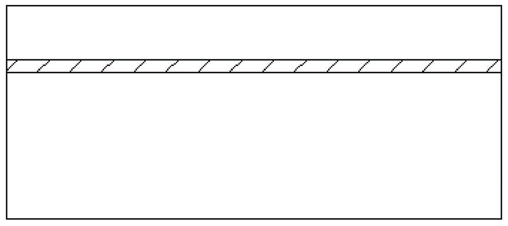
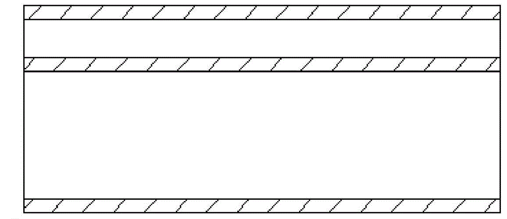
[0051] Specific implementation mode one: the following combination Figure 19 Describe this embodiment, a silicon microresonant pressure sensor core described in this embodiment adopts electrostatic excitation / piezoresistive detection as the working mode, and it includes a lower substrate 1 and an upper substrate 2, a lower substrate 1 and an upper substrate The substrate 2 is bonded as a whole;

[0052] The lower substrate 1 is provided with a resonant beam 1-1, a pressure sensitive diaphragm 1-2, a lower excitation electrode 1-3, a piezoresistor 1-4 and a lower lead pad 1-5; the upper part of the resonant beam 1-1 The surface is provided with the lower excitation electrode 1-3 and the varistor 1-4, and the leads of the lower excitation electrode 1-3 and the varistor 1-4 are drawn out through the lower lead pad 1-5; the pressure sensitive diaphragm 1-2 set at the bottom of the resonant cavity where the resonant beam 1-1 is located;

[0053] The upper substrate 2 is provided...

specific Embodiment approach 2

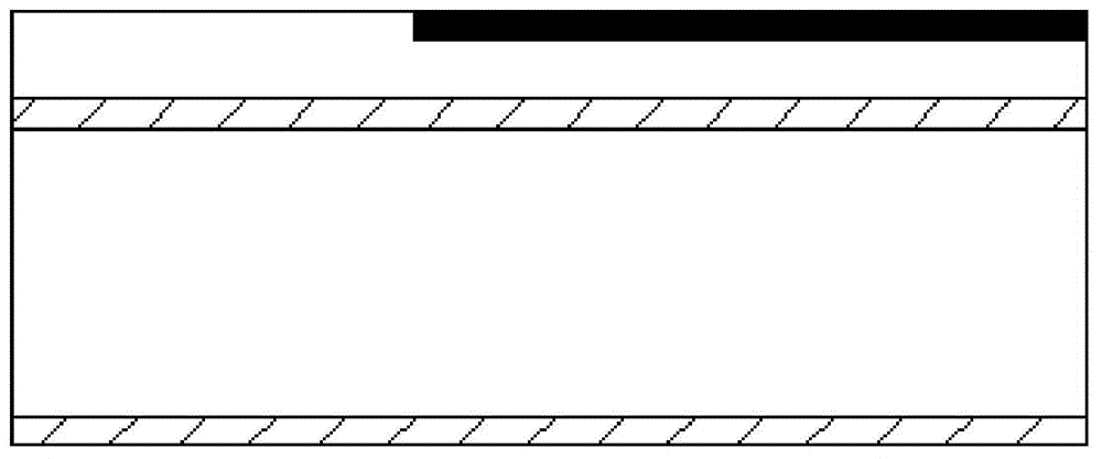
[0063] Specific implementation mode two: the following combination Figure 1 to Figure 19 Describe this embodiment, the method for making a silicon microresonant pressure sensor core described in Embodiment 1, the method includes the following steps:

[0064] Step 1, making the lower substrate, the specific process is:

[0065] Step 11, select SOI silicon wafer as the lower substrate to be processed, the SOI silicon wafer is provided with an intermediate oxide layer, and the intermediate oxide layer divides the SOI silicon wafer into upper and lower parts,

[0066] performing thermal oxidation treatment on the lower substrate to be treated, forming a silicon dioxide layer on the upper and lower surfaces of the lower substrate to be treated, and obtaining the thermally oxidized lower substrate;

[0067] Step 12, silicon dioxide is patterned by a photolithographic etching process, and then a varistor and its concentrated boron lead, a lower layer excitation electrode and its ri...


PUM

PropertyMeasurementUnit
Thicknessaaaaaaaaaa
Resistivityaaaaaaaaaa
Thicknessaaaaaaaaaa

Abstract

The invention discloses a silicon micro-resonance mode pressure sensor core and a manufacturing method, and belongs to the field of sensors, wherein the complex technologies such as silicon-silicon direct bonding and silicon slice thinning are not used, and large residual stress is prevented from being led in during the manufacturing process of harmonic oscillators. The silicon micro-resonance mode pressure sensor core comprises a lower layer substrate and an upper layer substrate, and the lower layer substrate and the upper layer substrate are bonded into a whole. The lower layer substrate is provided with a resonance beam, a pressure sensitive membrane, a lower layer exciting electrode, a voltage dependent resistor and a lower layer lead bonding pad. The lower layer exciting electrode and the voltage dependent resistor are arranged on the upper surface of the resonance beam. The pressure sensitive membrane is arranged at the bottom of a resonant cavity. An oscillating trough and an upper layer exciting electrode are arranged on the upper layer substrate, wherein the oscillating trough is formed in the lower surface of the upper layer substrate, and the upper layer exciting electrode covers the surface of the bottom of the oscillating trough. The oscillating trough formed in the lower surface of the upper layer substrate and the resonant cavity where the resonance beam is located form a closed space. The lower layer exciting electrode corresponds to the upper layer exciting electrode in position. An SOI silicon slice is selected and used as the lower layer substrate; a glass sheet is selected and used as the upper layer substrate.

Description

technical field [0001] The invention relates to a core body of a silicon micro-resonant pressure sensor and a manufacturing method thereof, belonging to the field of sensors. Background technique [0002] Silicon microresonant pressure sensors often use electrostatic excitation / piezoresistive detection, electrothermal excitation / piezoresistive detection, electromagnetic excitation / electromagnetic detection, and electrostatic excitation / capacitance detection. Compared with other working methods, electrostatic excitation / piezoresistive detection has the advantages of fast establishment speed, strong anti-interference ability of the detection method, small excitation heat generation, low power consumption, and easy miniaturization. However, in the existing manufacturing methods of silicon microresonant sensors, some of them are difficult to adopt this working method, and even some of them can be used, they also have their own shortcomings. [0003] For example, Greenwood et al...

Claims


Application Information

Patent Timeline
IPC IPC(8): G01L1/10G01L9/06
Inventor 吴亚林金建东王明伟李玉玲田雷吴紫峰刘智辉王永刚
Owner NO 49 INST CHINESE ELECTRONICS SCI & TECH GRP
Why Eureka
Try Eureka