
Channel voltage dividing field effect tube and production method based on high-energy ion implantation mode

A high-energy ion, field effect tube technology, applied in electrical components, semiconductor/solid-state device manufacturing, circuits, etc., can solve the problems of difficult production technology and process, and achieve the effect of eliminating capacitance, improving switching speed, and increasing doping concentration.

Active Publication Date: 2014-01-15
桂林斯壮桂微电子有限责任公司
View PDF4 Cites 5 Cited by
  • Summary
  • Abstract
  • Description
  • Claims
  • Application Information

AI Technical Summary

Problems solved by technology

However, most of Super Junction and 3D structures currently use single-layer molding methods. Due to the relatively difficult production technology, they are only in the hands of foreign brand manufacturers and a few domestic OEM companies.

Method used

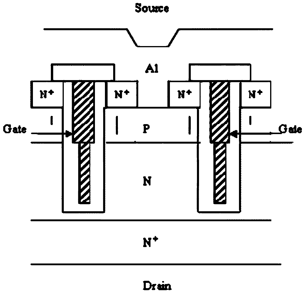

Image

  • Channel voltage dividing field effect tube and production method based on high-energy ion implantation mode
  • Channel voltage dividing field effect tube and production method based on high-energy ion implantation mode
  • Channel voltage dividing field effect tube and production method based on high-energy ion implantation mode

Examples


Embodiment Construction

[0026] A method for producing a channel pressure-dividing field-effect transistor based on high-energy ion implantation, characterized in that it includes the following steps:

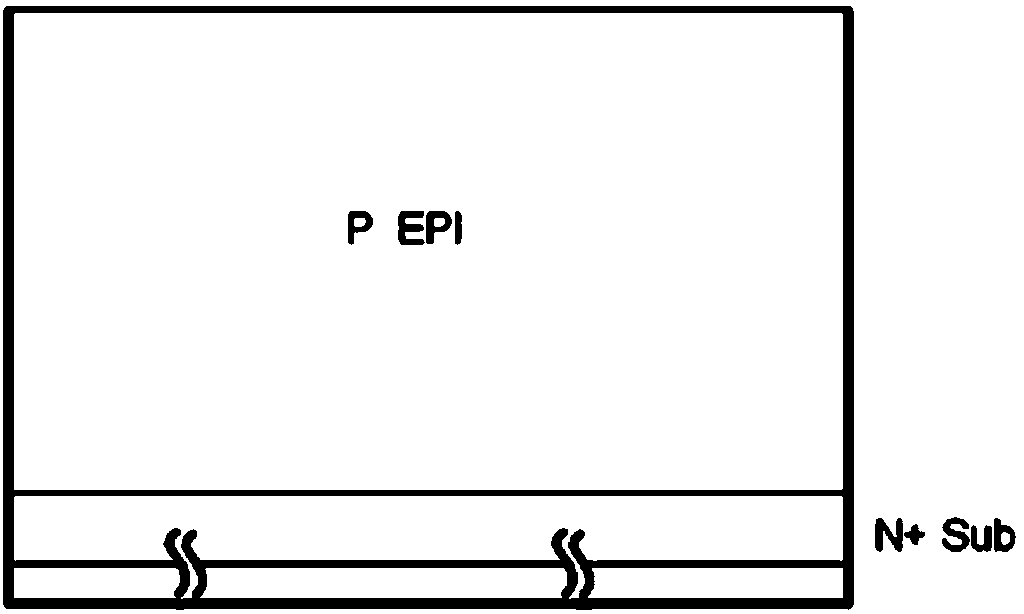
[0027] (1) growing a P-type epitaxial layer 5 on an N+ substrate 4; see figure 2 ;

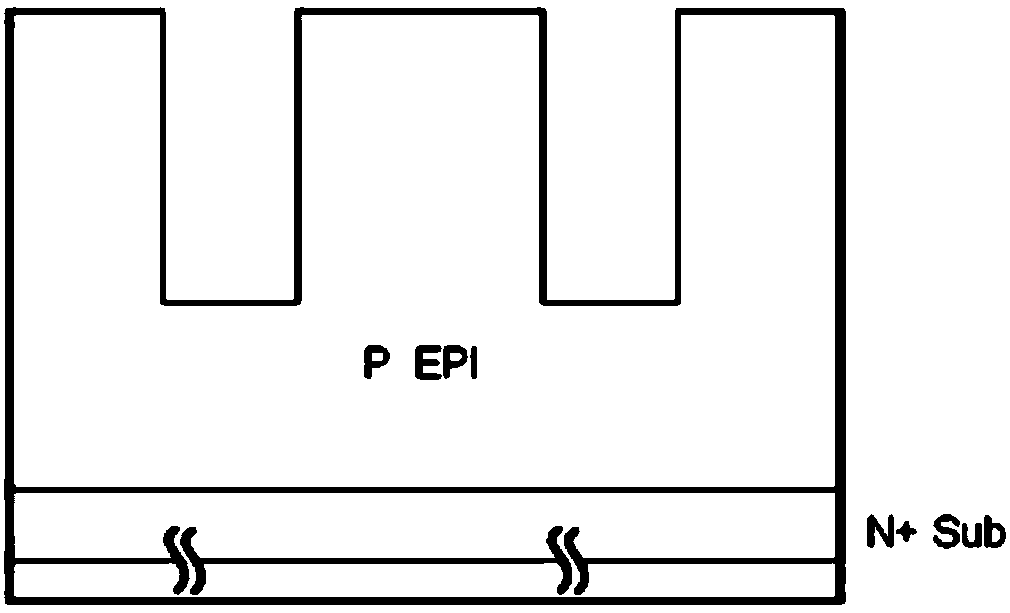
[0028] (2) Photoetching strip-shaped grooves on the P-type epitaxial layer 5 grown in step (1); see image 3 ; Among them, the photolithography stripe pattern is as Figure 3a shown;

[0029] (3) growing a silicon dioxide oxide layer on the groove wall, groove bottom, and the upper surface of the P-type epitaxial layer 5 obtained in step (2); see Figure 4 ;

[0030] (4) Deposit metal or polysilicon in the strip-shaped trench obtained in step (3) as a good conductor 8, and connect them together outside the functional area to form a gate 2; see Figure 5 ;

[0031] (5) Diffusion downward from the surface of the crystal obtained in step (4) to push the junction to form an n-region, see Figure 6 ;

[0032] (6) D...


PUM


Abstract

The invention discloses a channel voltage dividing field effect tube and production method based on a high-energy ion implantation mode. High-energy ion implantation equipment is used for carrying out gradual-deep implantation, an N-shaped channel is manufactured through diffusion for connecting a groove channel and a drain electrode, a similar-to-T-shaped structure formed by the N-shaped channel is of a 3D structure, a depletion zone formed between P and N is changed from a single vertical direction to a vertical direction and a horizontal direction, and accordingly the withstand voltage of the zone is greatly improved, the dosage concentration of the N channel can be increased, then the effect of lowering communicating resistance is achieved, and meanwhile P extends outwards and forms an obstruction between the bottom of a grid electrode and the drain electrode of the structure, and accordingly the capacitance between the bottom of the grid electrode and the drain electrode is nearly zero, the contacting part of the channel and the groove channel is small, so that the capacitance between the grid electrode and the drain electrode can be greatly removed, according to the two improvements, charging and discharging time during grid electrode opening and closing can be greatly shortened (Qgd can be greatly lowered), and accordingly opening and closing speed of an MOS tube is improved.

Description

technical field [0001] The invention relates to a power field effect tube, in particular to a channel partial pressure field effect tube based on high-energy ion implantation and a production method. Background technique [0002] When the back pressure of the power field effect (MOS) tube is high, because the epitaxial layer bears the back pressure, the resistivity of the epitaxial layer is relatively large and the thickness is relatively thick, resulting in the largest proportion of the resistance of the epitaxial layer to the overall on-resistance. Therefore, The effect of improving the performance of the power MOS tube by improving the resistance of the epitaxial layer is the most obvious. At present, the more popular method is to use a 3D structure similar to the Super Junction, such as figure 1 As shown, the 3D structure similar to Super Junction reduces the resistance of the epitaxial layer from two aspects. On the one hand, the space charge region that bears the bac...

Claims


Application Information

Patent Timeline
Patent Type & Authority Applications(China)
IPC IPC(8): H01L21/336H01L29/78H01L29/10
CPCH01L29/0634H01L29/0642H01L29/66666H01L29/7827
Inventor 关仕汉李勇昌彭顺刚邹锋王常毅
Owner 桂林斯壮桂微电子有限责任公司
Learn More