Method for manufacturing high-thermal-conductivity printed circuit board and printed circuit board
A technology for printed circuit boards and production methods, which is applied in the directions of printed circuit manufacturing, printed circuits, printed circuit components, etc., can solve the problem of poor thermal conductivity of printed circuit boards, immature use of printed circuit boards, and easy aluminum-based coating. To avoid problems such as falling off, to avoid the metal coating falling off, the electrical signal performance is superior, and the board space is saved.
- Summary
- Abstract
- Description
- Claims
- Application Information
AI Technical Summary
Problems solved by technology
Method used
Image
Examples
Embodiment 1
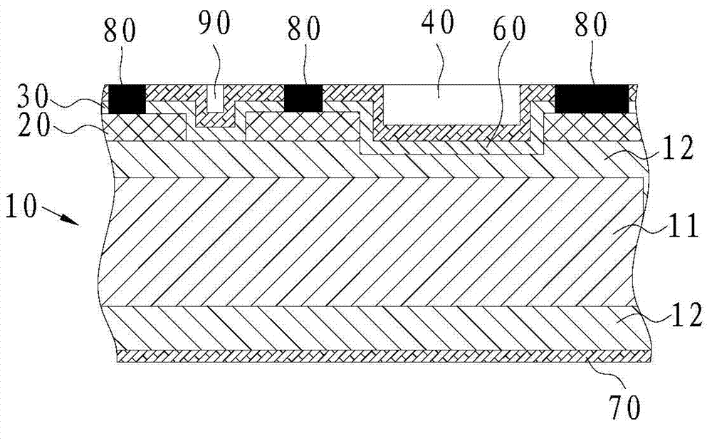
[0087] Such as figure 1 As shown, in this embodiment, the high thermal conductivity printed circuit board of the present invention includes a conductive layer 30, an adhesive sheet 20, and a substrate 10 arranged in sequence. The substrate 10 is a metal composite board, and the substrate 10 includes a Aluminum layer 11, a layer of copper layer 12 is provided on both sides of the aluminum layer 11, the thickness of the copper layer 12 is greater than 0.1mm, and the copper layer 12 provided on the side of the aluminum layer 11 is in contact with the adhesive sheet 20.
[0088] A power amplifier slot 40 for storing high-power electrical appliances and a blind hole 90 for heat dissipation are arranged on the conductive layer 30. The power amplifier slot 40 extends from the conductive layer 30 to the copper layer 12 close to the bonding sheet 20, and the blind hole 90 is formed by the conductive layer. 30 extends to the boundary line between the bonding sheet 20 and the substrate 1...
Embodiment 2
[0110] Such as Figure 13 As shown, in this embodiment, the high thermal conductivity printed circuit board of the present invention includes a conductive layer 300, an adhesive sheet 200 and a substrate 100 arranged in sequence, and the substrate 100 is a metal composite board. In this embodiment , the substrate 100 is an aluminum-copper composite board, the substrate 100 includes an aluminum layer 101, a layer of copper layer 102 is arranged on both sides of the aluminum layer 101, the thickness of the copper layer 102 is greater than 0.1mm, and the copper layer arranged on one side of the aluminum layer 101 102 is in contact with the adhesive sheet 200 .
[0111] A power amplifier slot 400 for storing high-power electrical appliances and a blind hole 900 for heat dissipation are arranged on the conductive layer 300. The power amplifier slot 400 and the blind hole 900 extend from the conductive layer 300 to the boundary line between the bonding sheet 200 and the substrate 10...
PUM
| Property | Measurement | Unit |
|---|---|---|
| thickness | aaaaa | aaaaa |
Abstract
Description
Claims
Application Information
 - Generate Ideas
- Intellectual Property
- Life Sciences
- Materials
- Tech Scout
- Unparalleled Data Quality
- Higher Quality Content
- 60% Fewer Hallucinations
Browse by: Latest US Patents, China's latest patents, Technical Efficacy Thesaurus, Application Domain, Technology Topic, Popular Technical Reports.
© 2025 PatSnap. All rights reserved.Legal|Privacy policy|Modern Slavery Act Transparency Statement|Sitemap|About US| Contact US: help@patsnap.com


