Homogeneous network growth web Growth epitaxy method on sic substrate

A substrate and mesh technology, which is applied in the field of homogeneous mesh growth and epitaxy of silicon carbide SiC substrate, can solve problems such as the influence of SiC device performance, and achieve the effect of increasing the film growth area and shortening the epitaxy time.

Active Publication Date: 2016-10-05
宁波合盛新材料有限公司
View PDF1 Cites 0 Cited by
  • Summary
  • Abstract
  • Description
  • Claims
  • Application Information

AI Technical Summary

Problems solved by technology

[0003] However, there are various defects in SiC that have a serious impact on device performance.

Method used


Image

  • Homogeneous network growth web Growth epitaxy method on sic substrate
  • Homogeneous network growth web Growth epitaxy method on sic substrate
  • Homogeneous network growth web Growth epitaxy method on sic substrate

Examples


Embodiment Construction

[0023] The technical solutions of the present invention will be described in further detail below with reference to the accompanying drawings and embodiments.

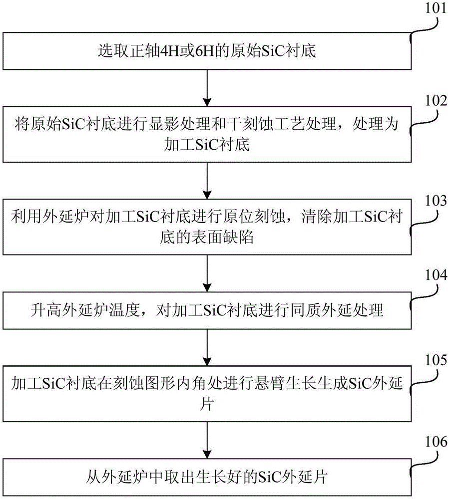
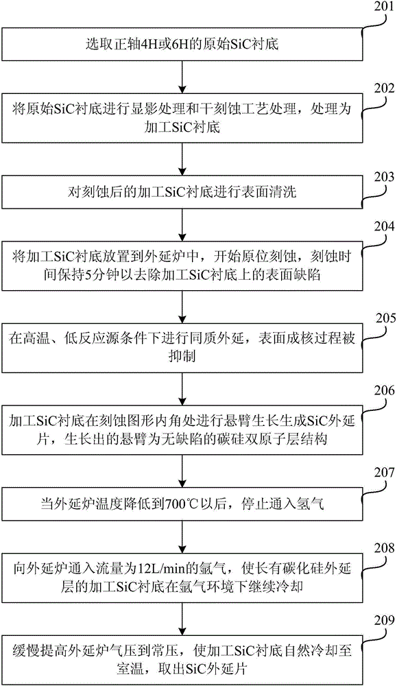
[0024] figure 1 It is a flow chart of Embodiment 1 of the SiC substrate homogeneous Web Growth epitaxy method of the present invention. As shown in the figure, this embodiment specifically includes:

[0025] Step 101, selecting an original SiC substrate with positive axis 4H or 6H;

[0026] In step 102, the original SiC substrate is subjected to development treatment and dry etching process to process the SiC substrate; the SiC substrate becomes a mesa, and the etching area is the area of ​​the device to be manufactured, and the etching depth is 5um to 20um. The table has six spindles;

[0027] Step 103, using an epitaxy furnace to perform in-situ etching on the processed SiC substrate to remove surface defects on the processed SiC substrate;

[0028] Step 104, increasing the temperature of the epitaxial furnace, an...


PUM

PropertyMeasurementUnit
angleaaaaaaaaaa

Abstract

The invention relates to a SiC substrate homogeneous Web Growth epitaxy method. The method comprises the steps of choosing a positive-axis 4H or 6H original SiC substrate, carrying out developing process and dry etching process on the original SiC substrate to obtain a processed SiC substrate, utilizing an epitaxy furnace to carry out in-situ etching on the processed SiC substrate, carrying out homogeneous epitaxy processing on the processed SiC substrate, carrying out cantilever growth at the inner corner position of an etched pattern of the processed SiC substrate to generate a SiC epitaxy wafer, regrowing a grown cantilever into a layer of carbon silicon double-atomic-layer film to cover an etched tabletop area, and taking the grown SiC epitaxy wafer out of the epitaxy furnace. The grown cantilever is of a non-defective carbon silicon double-atomic-layer structure. According to the SiC substrate homogeneous Web Growth epitaxy method, a layer of thin complete non-defective cantilever is formed in an etching tabletop of the top end of the positive-axis silicon carbide substrate in an extending mode. Furthermore, epitaxy time is effectively shortened, and the film growth area is improved.

Description

technical field [0001] The invention relates to the technical field of semiconductor materials, in particular to a homogeneous web growth (Web Growth) epitaxy method on a silicon carbide SiC substrate Background technique [0002] As one of the representatives of wide band gap semiconductor materials, silicon carbide SiC has superior properties such as large band gap, high breakdown electric field, high thermal conductivity, high electron saturation drift velocity, strong radiation resistance and good chemical stability. It has become a key semiconductor material for the manufacture of a new generation of microelectronic devices and circuits after germanium, silicon, and gallium arsenide. Compared with Si-based devices under the same conditions, SiC-based devices can withstand much higher voltage and microwave power. For example, the ft of SiC MESFET can reach 12-15GHz. [0003] However, there are various defects in SiC that seriously affect the device performance. SiC sub...

Claims


Application Information

Patent Timeline
Patent Type & Authority Patents(China)
IPC IPC(8): H01L21/20C30B25/16
CPCC30B25/186C30B25/20H01L21/02378H01L21/02529H01L21/02634H01L21/02658H01L21/02661
Inventor 贾仁需辛斌宋庆文张艺蒙闫宏丽
Owner 宁波合盛新材料有限公司
Why Eureka
Try Eureka