Method for preparing gluing component
A component and gluing technology, applied in the field of optical glue, can solve problems such as bubbles on the edge of decorative ink
- Summary
- Abstract
- Description
- Claims
- Application Information
AI Technical Summary
Problems solved by technology
Method used
Image
Examples
preparation example Construction
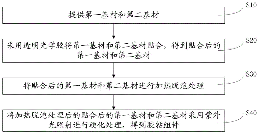
[0033] Such as figure 1 Shown, the preparation method of the adhesive assembly of an embodiment, comprises the following steps:
[0034] S10, providing a first base material and a second base material.
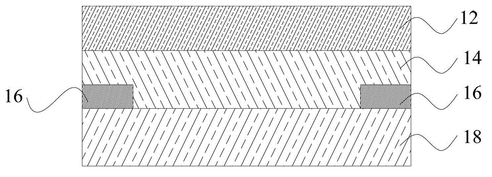
[0035] The first base material and the second base material refer to parts that need to be bonded with transparent optical adhesive. In the touch screen field, the first substrate is a panel, and the second substrate is a sensor circuit.
[0036] S20. Bonding the first base material and the second base material by using transparent optical adhesive to obtain the bonded first base material and the second base material.
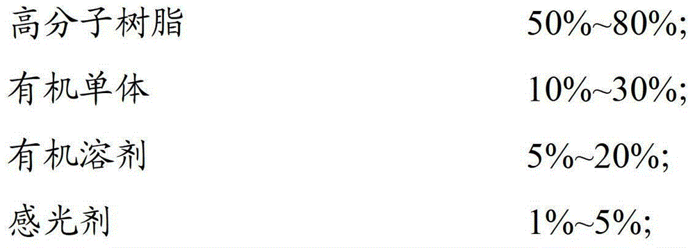
[0037] Transparent optical glue includes the following components in the following weight percentages:
[0038]
[0039] The polymer resin may be selected from at least one of acrylate polymer, epoxy resin and polyvinyl ether.
[0040] The organic monomer may be selected from at least one of acrylate and vinyl ether.
[0041] The organic solvent may be ...
Embodiment 1
[0059] Add 50 g of polymethyl methacrylate, 29 g of ethyl acrylate and 1 g of quinone diazide into 20 g of tetrahydrofuran solution, and mix well to prepare transparent optical adhesive 1. After laminating the panel and the sensor circuit with transparent optical adhesive 1, defoaming treatment was performed at 40°C and a pressure of 0.65Mpa for 40 minutes to remove the air bubbles in the transparent optical adhesive 1. Next, use a wavelength of 365nm and an energy of 3000mj / cm 2 The ultraviolet light irradiates the transparent optical adhesive to harden the transparent optical adhesive 1 . The electronic device obtained after laminating the panel and the sensor circuit with the transparent optical adhesive 1 has almost no air bubbles and has a flat surface.
Embodiment 2
[0061] Add 80g polymethyl methacrylate, 10g ethyl ethacrylate and 3.8g diazonaphthoquinonesulfonyl chloride to 5g cyclohexanone, then add 0.5g p-methoxyphenol, 0.2g diisononyl phthalate ester and 0.5g of fatty acid ester, mixed evenly to prepare transparent optical adhesive 2. After laminating the panel and the sensor circuit with transparent optical adhesive 2, defoaming treatment was performed at 80°C and a pressure of 0.6Mpa for 10 minutes to remove air bubbles in the transparent optical adhesive 2. Next, use a wavelength of 365nm and an energy of 500mj / cm 2 The ultraviolet light is irradiated to the transparent optical adhesive to harden the transparent optical adhesive 2 . The electronic device obtained after laminating the panel and the sensor circuit with the transparent optical adhesive 2 has almost no bubbles and a flat surface.
PUM
| Property | Measurement | Unit |
|---|---|---|
| wavelength | aaaaa | aaaaa |
| thickness | aaaaa | aaaaa |
Abstract
Description
Claims
Application Information
 - R&D
- Intellectual Property
- Life Sciences
- Materials
- Tech Scout
- Unparalleled Data Quality
- Higher Quality Content
- 60% Fewer Hallucinations
Browse by: Latest US Patents, China's latest patents, Technical Efficacy Thesaurus, Application Domain, Technology Topic, Popular Technical Reports.
© 2025 PatSnap. All rights reserved.Legal|Privacy policy|Modern Slavery Act Transparency Statement|Sitemap|About US| Contact US: help@patsnap.com


