A flexible surface-enhanced Raman spectroscopy substrate and its preparation method
A surface-enhanced Raman and substrate technology, which is used in Raman scattering, processes for producing decorative surface effects, and fabrication of microstructure devices, etc. and analysis of environmental universality and other issues, to achieve the effect of saving economic costs, macro universality and generalizability
- Summary
- Abstract
- Description
- Claims
- Application Information
AI Technical Summary
Problems solved by technology
Method used
Image

Examples
Embodiment 1
[0029] Embodiment 1, preparation of flexible gold reinforced substrate
[0030] 1) Sacrificial template substrate cleaning: the silicon wafer substrate with a 300nm oxide layer used as a sacrificial template was ultrasonically cleaned in water, acetone, absolute ethanol and deionized water for 10 minutes, and then treated with an oxygen plasma cleaner to obtain a surface Clean hydrophilic silicon substrate.
[0031] 2) Metal active layer deposition: use vacuum thermal evaporation to deposit a uniform gold film on the surface of the substrate: put the substrate prepared in step 1) into the vacuum thermal evaporation coating system, and select the evaporation source with a purity of 99.999% % gold wire, vacuumed to about 10 3 After Pa, the control current is The rate of vapor deposition of gold film. Through a series of comparative experiments with gold film thicknesses of 0, 1, 3, 5, 8, 10, 15 and 20nm, it was found that the gold film thickness of 8nm can obtain the best en...
Embodiment 2
[0034] Example 2. Preparation of a flexible silver-reinforced substrate.
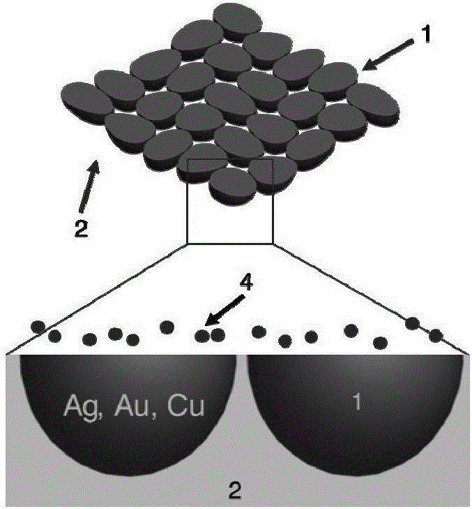
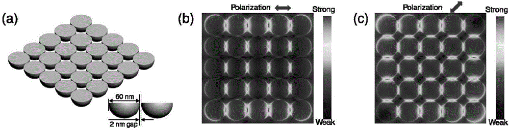
[0035] The preparation method is basically the same as that in Example 1, the difference is that in step 2), 99.999% silver bars are used as the evaporation source, and the SEM and TEM morphology characterization of the silver film is shown in Figure 5 (d), Figure 5 (e) and Figure 5 (f), it can be seen that the silver film is a discrete island structure, most of the gaps are about 5-10nm in size, but there are also many small gap structures with local gaps of 2-3nm, which meet the conditions for the formation of ideal electromagnetic enhancement effects, The extinction spectra in the visible region of gold films with different thicknesses are shown in Figure 4 (b); the baking condition in step 3) is 100°C for 10 min; after removing the sacrificial template in step 4), the SEM characterization results of the flexible silver-reinforced substrate are shown in Figure 7 (b). On the other hand, the s...
Embodiment 3
[0036] Embodiment 3, preparation and detection of flexible silver reinforced substrate
[0037] 1) Cleaning of the base of the sacrificial template: After rinsing the clean and flat aluminum foil with ethanol, set it aside.
[0038] 2) Silver active layer deposition: Step 1) The aluminum foil is put into a vacuum thermal evaporation coating system, and the silver evaporation source is a silver bar with a purity of 99.999%. Vacuum down to about 10 3 After Pa, the control current is The gold film is evaporated and deposited at a rate of 8nm, and the thickness indicated by the instrument (monitored by the crystal oscillator) is 8nm, and the composite structure of the medium layer / silver active layer supported by the sacrificial template is obtained.
[0039] 3) Encapsulation of the support layer: same as in Example 1, the baking condition is 100° C. for 10 minutes, and the thickness of the support layer is about 300 nm.
[0040] 4) Removal of the sacrificial template: 50 mL o...
PUM
| Property | Measurement | Unit |
|---|---|---|
| thickness | aaaaa | aaaaa |
| thickness | aaaaa | aaaaa |
| thickness | aaaaa | aaaaa |
Abstract
Description
Claims
Application Information
 - R&D
- Intellectual Property
- Life Sciences
- Materials
- Tech Scout
- Unparalleled Data Quality
- Higher Quality Content
- 60% Fewer Hallucinations
Browse by: Latest US Patents, China's latest patents, Technical Efficacy Thesaurus, Application Domain, Technology Topic, Popular Technical Reports.
© 2025 PatSnap. All rights reserved.Legal|Privacy policy|Modern Slavery Act Transparency Statement|Sitemap|About US| Contact US: help@patsnap.com