Brazed layer predeposition method

A pre-deposition and brazing layer technology, applied in welding equipment, electrical components, circuits, etc., can solve the problems of poor uniformity of solder paste or solder melting degree, poor consistency of welding quality, inaccurate alignment, etc. Good uniformity, reduced processing workload, and high thickness uniformity

Active Publication Date: 2013-08-28
CHINA ELECTRONIS TECH INSTR CO LTD
View PDF7 Cites 4 Cited by
  • Summary
  • Abstract
  • Description
  • Claims
  • Application Information

AI Technical Summary

Problems solved by technology

[0004] No matter using solder paste or brazing connection with solder sheet, the coating amount of solder paste or the size, shape and thickness of solder sheet cannot be precisely controlled. Under the same welding parameters, the uniformity of solder paste or solder melting degree is poor, resulting in module or Poor consistency of welding quality everywhere in the assembly;
[0005] Solder paste or solder sheet welding, there is a problem of alignment between the soldering position, solder paste or solder sheet, and the hybrid integrated circuit chip to be soldered. Whether using equipment alignment or manual alignment, the alignment accuracy is not It cannot meet the needs of high-precision and high-density welding, especially when it is transferred to the heating process after alignment, the relative displacement between the three will be caused by turnover or movement, and eventually lead to waste products caused by inaccurate alignment

Method used


Image

  • Brazed layer predeposition method
  • Brazed layer predeposition method

Examples


Embodiment 1

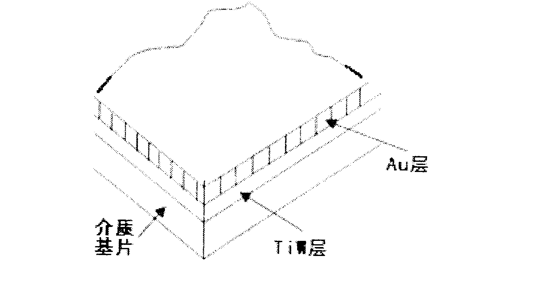
[0030] Such as Figure 1 to Figure 2 As shown, the technical scheme of the present invention takes the electroplating pre-deposition of gold-tin eutectic solder commonly used in hybrid integrated circuits as an example, and the scheme adopts the scheme of electroplating multiple layers of gold and tin layers, so that the two components of gold and tin The uniformity of the alloy composition is as close as possible to the uniformity of the alloy composition. The implementation process in the scheme is as follows:

[0031] Vacuum sputtering coating seed layer:

[0032] In this scheme, the deposition of the adhesion layer and the electroplating seed layer on the welding surface of the hybrid integrated circuit adopts the method of magnetron sputtering, and successively deposits the adhesion layer (such as TiW layer) and the electroplating seed layer on the dielectric substrate of the hybrid integrated circuit respectively. layer (eg Au layer), such as figure 1 shown;

[0033] ...

Embodiment 2

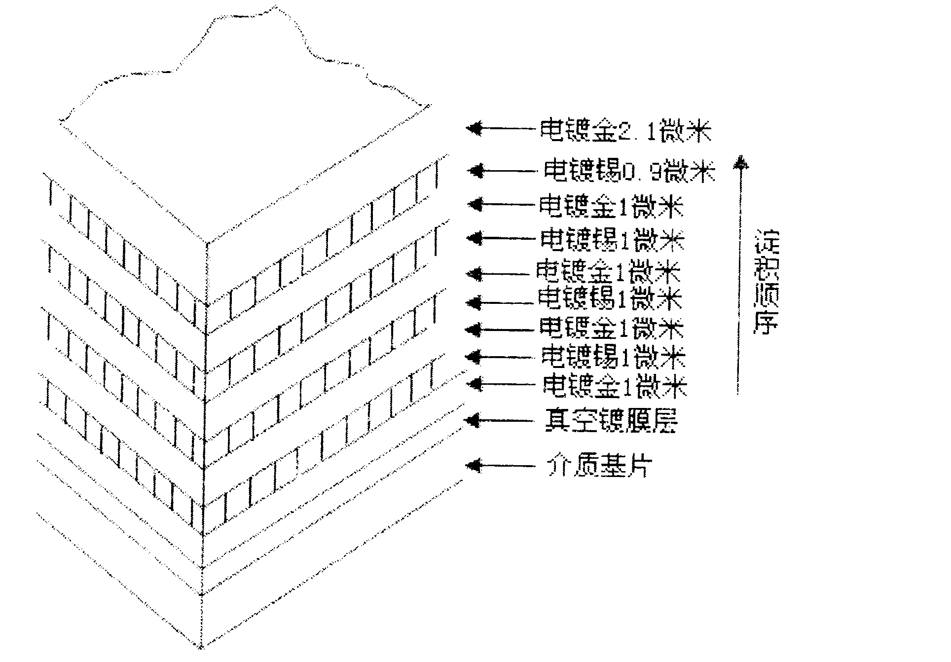
[0036] On the basis of the above embodiments, further, a brazing layer pre-deposition method of the present invention, which includes the following steps:

[0037] A: Vacuum sputtering coating seed layer;

[0038] B: Each layer is deposited by alternate electroplating of gold and tin layers in sequence.

[0039] Preferably, in the step A, the adhesion layer and the electroplating seed layer are sequentially deposited on the circuit dielectric substrate by using the method of magnetron sputtering, which is a solution that can be realized in the prior art.

[0040] Preferably, the circuit dielectric substrate is a hybrid integrated circuit dielectric substrate.

[0041] Preferably, in the step B, the density of gold is 19.3g / cm3; the density of tin is 7.31g / cm3, here, the density of gold can also be 20.3g / cm3; the density of tin is 8.31g / cm3.

[0042] Preferably, in the step B, the weight ratio of gold and tin is 80.4:19.6, here the weight ratio can also be 80.7:19.3, and the ...


PUM

PropertyMeasurementUnit
Densityaaaaaaaaaa
Densityaaaaaaaaaa
Densityaaaaaaaaaa

Abstract

The invention provides a brazed layer predeposition method, which comprises the following steps: A: vacuum sputtering coating a seed layer, and B: depositing each layer through a manner of sequentially alternating a gold layer and a tin layer. Through the scheme, the brazed layer predeposition method not only solves the problems existed in the prior art, and has the obvious advantages that aiming at a hybrid integrated circuit adopting braze, a process method by adopting soldering paste or soldering flux pieces in traditional soldering is improved, a layer of soldering flux layer with each component weight ratio being equivalent to components of the soldering flux pieces is deposited on a circuit soldering face (generally refers to a back face), the circuit can be directly placed on a soldering position when soldering is carried out, and soldering is realized through heating. Due to the technology, the processing workload for forming the soldering flux pieces can be reduced, and wastes caused by position offset among soldering positions, the soldering flux pieces, and the circuit to be soldered when soldering is carried out can be reduced.

Description

technical field [0001] The invention relates to the field of brazing assembly of hybrid integrated circuits, in particular to a method for pre-depositing a brazing layer. Background technique [0002] At present, hybrid integrated circuits are widely used in high reliability, high thermal conductivity and high electrical conductivity. The brazing assembly technology of hybrid integrated circuits is also receiving more and more attention. The quality of soldered chips of hybrid integrated circuits directly affects the circuit Whether it has high reliability, high thermal conductivity and high electrical conductivity. [0003] The brazing process of hybrid integrated circuits, one method is to apply solder paste to the welding position, then place the hybrid integrated circuit on the solder paste with a placement machine, melt the solder paste by heating, and realize the brazing connection after cooling; Another method is to use solder sheet, cut the solder sheet to be the sa...

Claims


Application Information

Patent Timeline
IPC IPC(8): B23K1/20H01L21/60
Inventor 王斌路波宋振国樊明国
Owner CHINA ELECTRONIS TECH INSTR CO LTD
Why Eureka
Try Eureka