
Ultraviolet selective silicon avalanche photoelectric detection chip

A selective, chip-based technology, applied in circuits, electrical components, semiconductor devices, etc., can solve the problems of high difficulty in making substrate materials, chip manufacturing process, difficulty in mass production, and high cost, and achieve the effect of avalanche multiplication

Inactive Publication Date: 2013-07-17
SOUTH WEST INST OF TECHN PHYSICS
View PDF7 Cites 9 Cited by
  • Summary
  • Abstract
  • Description
  • Claims
  • Application Information

AI Technical Summary

Problems solved by technology

The above devices are basically compound semiconductor ultraviolet detectors. Due to the difficulty in manufacturing substrate materials and the special chip manufacturing process, it is difficult to achieve mass production and the cost is high.

Method used


Image

  • Ultraviolet selective silicon avalanche photoelectric detection chip
  • Ultraviolet selective silicon avalanche photoelectric detection chip

Examples


Embodiment Construction

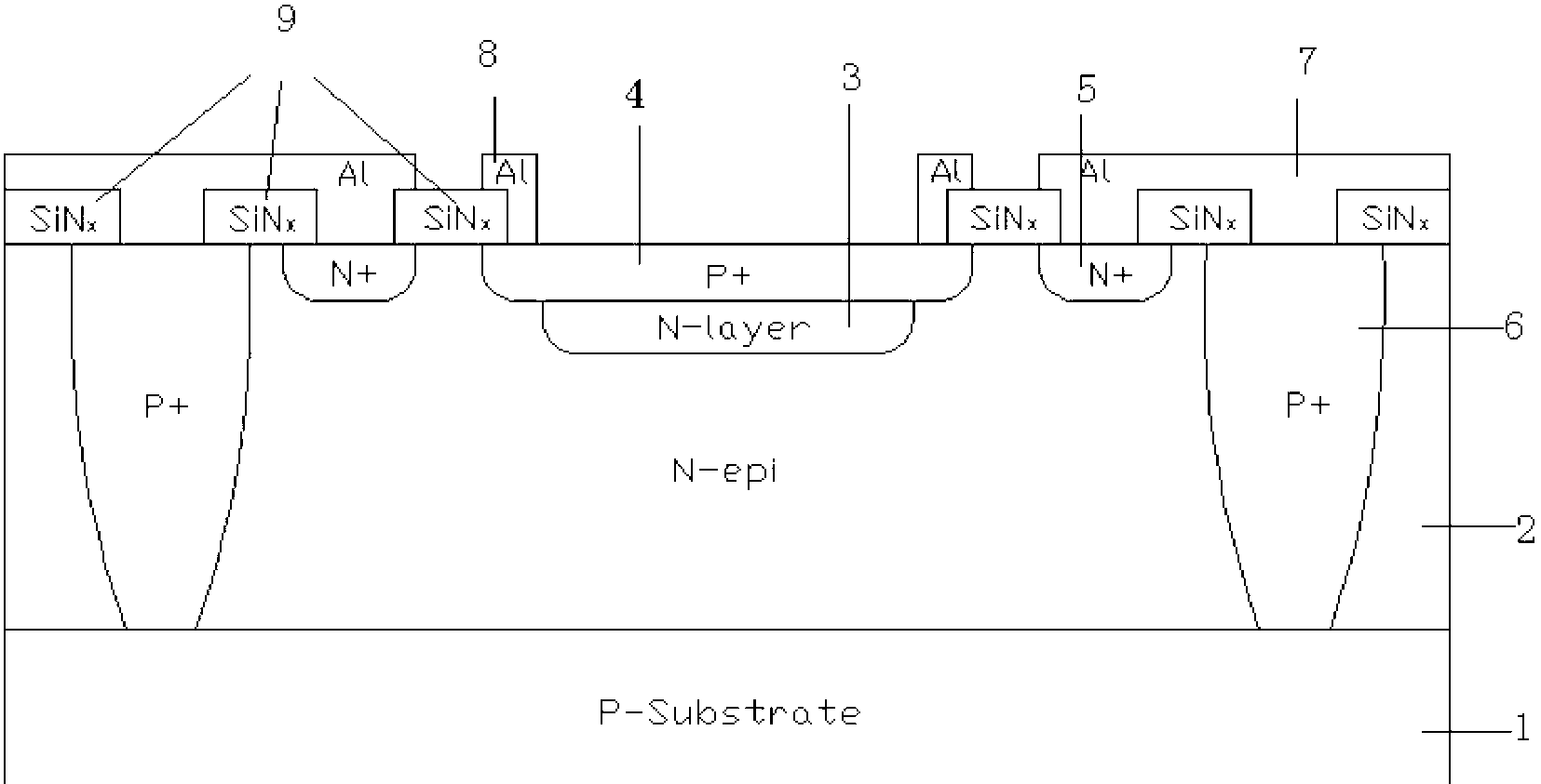
[0013] refer to figure 1 . First, according to the calculation of the absorption coefficient of silicon materials in the ultraviolet (λ≤400 nm) band, the absorption length of silicon materials in the ultraviolet wavelength λ≤400 nm band is less than 0.1 μm. In order to achieve high quantum efficiency detection of silicon in the ultraviolet band, the thickness of the light-absorbing layer 4 must be greater than 100 nm, so as to prevent the photo-generated carriers from entering the high-field N-type layer in the reverse-biased depletion state before recombining near the surface 3. Under the acceleration of the electric field, a collision ionization effect is generated to realize the avalanche multiplication of photogenerated carriers. Secondly, considering the absorption of silicon materials beyond the wavelength range of ultraviolet λ≤400 nm, this embodiment designs P + The deep diffusion region 6 penetrates the entire N - epitaxial layer 2, and the P connected to the N+ oh...


PUM

PropertyMeasurementUnit
Resistivityaaaaaaaaaa
Thicknessaaaaaaaaaa
Thicknessaaaaaaaaaa

Abstract

The invention provides an ultraviolet selective silicon avalanche photoelectric detection chip. A P+ light absorption layer (4) with the thickness of smaller than 200nm is connected with an N-type layer (3), An N+ ohmic contact layer (5) is symmetrical to the P+ light absorption layer (4), high-doping deep-diffusion regions penetrating through a whole N-type epitaxial layer (2) are arranged on two sides of the N+ ohmic contact layer (5) so as to enable the whole chip outside an avalanche region to be located in a P+ deep diffusion region (6) with the same potential as the chip, the P+ deep diffusion region (6) is connected with the N+ ohmic contact layer (5) through a silicon nitride passivation layer (9) arranged on an upper-end plane of the N-type epitaxial layer (2), a chip positive pole (7) and a chip negative pole (8). The ultraviolet selective silicon avalanche photoelectric detection chip avoids composition of a photon-generated carrier on the surface through the ultra-thin light absorption layer, produces the collision ionization effect under the acceleration effect of an electric field and achieves avalanche multiplication of the photon-generated carrier. The high-doping deep-diffusion regions penetrate through the whole epitaxial layer, so that the selective detection of an ultraviolet band is achieved.

Description

technical field [0001] The invention belongs to the field of ultraviolet imaging technology and relates to a chip structure of an ultraviolet selective silicon avalanche photodetector. Background technique [0002] UV photodetector is the core key component of UV detection technology such as UV alarm. The ultraviolet warning is to use the ultraviolet band of the "solar spectral blind zone" to detect the flame and tail flame of the missile. Since the UV warning system avoids the complex background caused by the sun, the most powerful natural light source, the "solar spectral blind" UV warning provides an extremely effective means of approach warning. At present, ultraviolet warning equipment has developed into one of the largest approach warning systems equipped. The development of high-sensitivity and low-noise ultraviolet detection devices is an important basic work for ultraviolet warning equipment. [0003] For silicon materials, the absorption coefficient α in the ult...

Claims


Application Information

Patent Timeline
IPC IPC(8): H01L31/107
Inventor 周红轮刘小会曾璞
Owner SOUTH WEST INST OF TECHN PHYSICS
Learn More