Electronic device housing integrating antenna and manufacturing method of the housing

A technology for electronic devices and manufacturing methods, which are applied to antenna supports/mounting devices, electrical components, transmission systems, etc., to achieve the effects of reducing manufacturing processes, increasing overall surface area, and reducing manufacturing costs

Inactive Publication Date: 2013-07-10
ACER INC
View PDF3 Cites 0 Cited by
  • Summary
  • Abstract
  • Description
  • Claims
  • Application Information

AI Technical Summary

Problems solved by technology

[0005] In view of this, the main purpose of the present invention is to provide an electronic device housing structure with integrated antenna and its manufact...

Method used


Image

  • Electronic device housing integrating antenna and manufacturing method of the housing
  • Electronic device housing integrating antenna and manufacturing method of the housing
  • Electronic device housing integrating antenna and manufacturing method of the housing

Examples


Embodiment Construction

[0028] In order to better understand the technical content of the present invention, a preferred embodiment is given and described as follows.

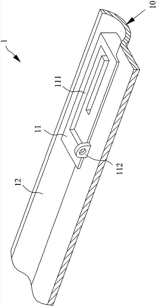
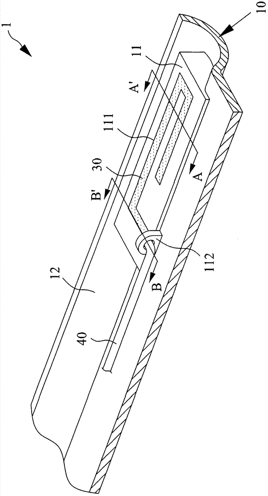
[0029] Please also refer to figure 1 and figure 2 . figure 1 It is a schematic diagram of the shell structure 10 of the electronic device shell 1 integrating the antenna of the present invention; figure 2 It is a schematic diagram of forming a three-dimensional antenna structure 30 with the casing structure 10 of the housing 1 of the integrated antenna of the present invention. In one embodiment of the present invention, the antenna-integrated electronic device casing 1 can be applied to a portable computer, but the present invention is not limited thereto, and can also be applied to smart phones, personal digital assistants, or other devices that require an antenna. Portable electronic devices, etc.

[0030] Such as figure 1 As shown, the antenna-integrated electronic device casing 1 of the present invention includes a casing ...


PUM


Abstract

An electronic device housing integrating an antenna and a manufacturing method of the housing. The method comprises the following steps: providing a housing including a model structure which is arranged on an inner surface of the housing in a protruding manner and includes a recessed part; spraying metal material on the model structure and enabling metal material to be filled in the recessed part; and removing redundant metal material located on the surface of the model structure, so as to enable the metal material in the recessed part to form a stereoscopic antenna structure. The invention also provides an electronic device housing manufactured by using the abovementioned manufacturing method of the electronic device housing integrating an antenna. Through the design of the electronic device housing integrating an antenna, the metal material forms an antenna in a stereoscopic form through the model structure of a housing structure, compared with an existing antenna by laser engraving, the antenna itself formed in the invention can provide an overall superficial area of a greater range by changing the depth of the recessed part, and the existing relatively complicated antenna manufacturing process can be reduced, so as to reduce manufacturing cost.

Description

technical field [0001] The invention relates to an electronic device casing, in particular to an electronic device casing integrated with an antenna and a manufacturing method thereof. Background technique [0002] All portable electronic devices are equipped with antenna components to provide the device with the ability to send and receive wireless communication signals or transmit data. Generally, the antenna assembly itself has a certain volume. For portable electronic devices that tend to be thinner and lighter, the internal space is limited. Therefore, issues such as space and circuit configuration must be considered when installing the antenna, which is inconvenient for device manufacturing or assembly. With the advancement of science and technology, an antenna structure made of laser engraving and molding technology (LDS) has gradually been developed, which can directly engrave the desired antenna pattern on the surface of the housing, and then electroplate the antenn...

Claims


Application Information

Patent Timeline
IPC IPC(8): H01Q1/22H04B1/08
Inventor 郭彦麟林永森
Owner ACER INC
Why Eureka
Try Eureka