Resin composition for forming optical waveguide and optical waveguide using the composition
A resin composition and optical waveguide technology, applied in the field of optical waveguides, can solve the problems of sacrificing flexibility, viscosity, increase in refractive index of cladding, deterioration of optical loss, etc., to improve viscosity, improve bending loss, and maintain low refractive index. Effect
- Summary
- Abstract
- Description
- Claims
- Application Information
AI Technical Summary
Problems solved by technology
Method used
Image
Examples
Embodiment 1
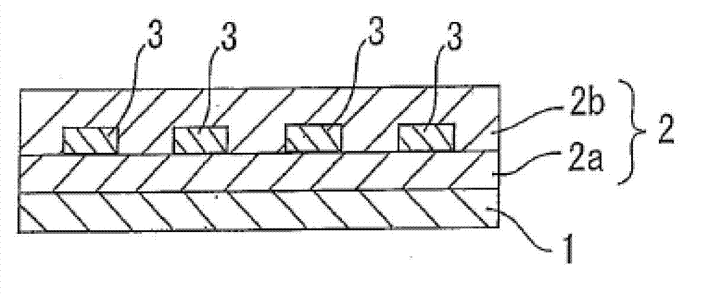
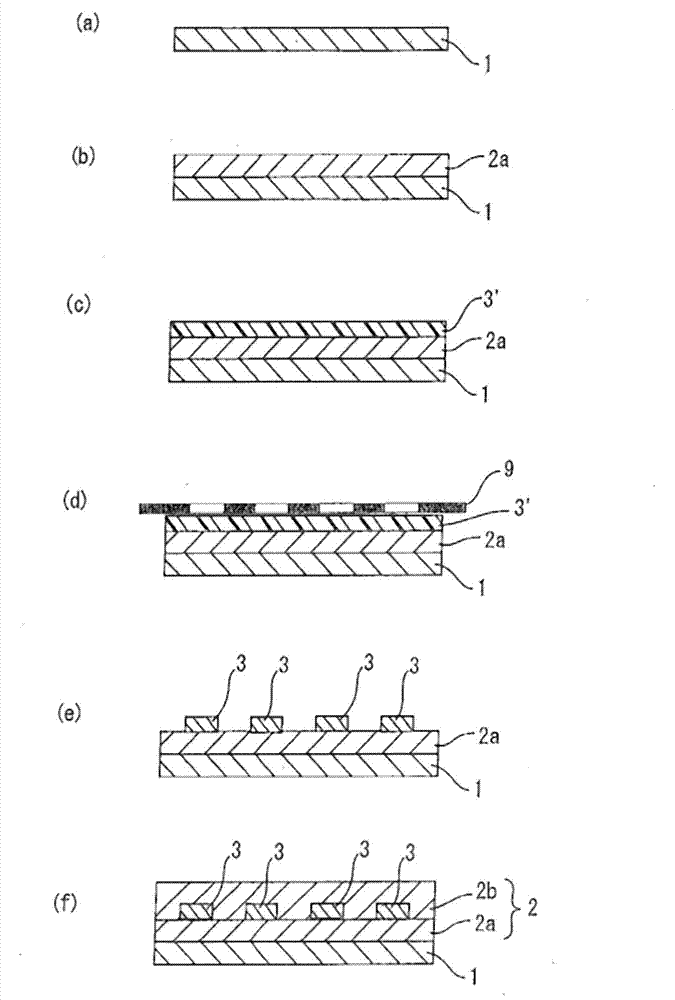
[0059] First, before fabricating the optical waveguide of the example, each photosensitive varnish as a cladding layer forming material and a core layer forming material was prepared.
[0060] Preparation of cladding-forming materials
[0061] Under light-shielding conditions, mix 30 g of polyvinyl butyral in 233 g of cyclohexanone [manufactured by Sekisui Chemical Co., Ltd., S-LEC BM-1: in formula (1), R=-C 3 h 7 , k=65±3, m=3 or less, n=about 34, weight average molecular weight 40000], 35g of urethane acrylate resin (manufactured by Mitsubishi Chemical Corporation, UA-160TM), 35g of trimethylolpropane (EO ) triacrylate resin (manufactured by Sanyo Chemical Co., Ltd., TA-401), 1.0 g of IRGACURE 819 (manufactured by Ciba Japan K.K.) and 3.0 g of IRGACURE 127 (manufactured by Ciba Japan K.K.) as photoradical polymerization initiators, and in It was stirred under heating at 85°C to dissolve it completely, then cooled to room temperature (25°C), and then heated and pressure-f...
Embodiment 2
[0072] When preparing the photosensitive varnish as the cladding material, the resin component ratio was changed to 40g of polyvinyl butyral (manufactured by Sekisui Chemical Co., Ltd., S-LECBM-1), 30g of urethane acrylate resin (manufactured by Mitsubishi Chemical Corporation, UA-160TM), 30 g of trimethylolpropane (EO) triacrylate resin (manufactured by Sanyo Chemical Corporation, TA-401). In the same manner as in Example 1 except for this, an optical waveguide in which a lower cladding layer was formed on a silicon wafer substrate, a core layer with a predetermined pattern was formed on the lower cladding layer, and an upper cladding layer was formed on the core layer was manufactured. .
Embodiment 3
[0074] When preparing the photosensitive varnish as the cladding material, the resin component ratio was changed to 50 g of polyvinyl butyral (manufactured by Sekisui Chemical Co., Ltd., S-LECBM-1), 25 g of urethane acrylate resin (manufactured by Mitsubishi Chemical Corporation, UA-160TM), 25 g of trimethylolpropane (EO) triacrylate resin (manufactured by Sanyo Chemical Corporation, TA-401). In the same manner as in Example 1 except for this, an optical waveguide in which a lower cladding layer was formed on a silicon wafer substrate, a core layer with a predetermined pattern was formed on the lower cladding layer, and an upper cladding layer was formed on the core layer was manufactured. .
PUM
| Property | Measurement | Unit |
|---|---|---|
| refractive index | aaaaa | aaaaa |
| refractive index | aaaaa | aaaaa |
| refractive index | aaaaa | aaaaa |
Abstract
Description
Claims
Application Information
 - R&D
- Intellectual Property
- Life Sciences
- Materials
- Tech Scout
- Unparalleled Data Quality
- Higher Quality Content
- 60% Fewer Hallucinations
Browse by: Latest US Patents, China's latest patents, Technical Efficacy Thesaurus, Application Domain, Technology Topic, Popular Technical Reports.
© 2025 PatSnap. All rights reserved.Legal|Privacy policy|Modern Slavery Act Transparency Statement|Sitemap|About US| Contact US: help@patsnap.com


