Vertical double-diffused field-effect tube and manufacturing process thereof

A vertical double-diffusion and field effect transistor technology, which is applied in semiconductor/solid-state device manufacturing, electrical components, circuits, etc., can solve problems such as leakage and breakdown voltage drop, so as to solve the problem of leakage, breakdown voltage will not drop, The effect of reducing production costs

Active Publication Date: 2013-06-12
HANGZHOU SILICON-MAGIC SEMICON TECH CO LTD
View PDF3 Cites 12 Cited by
  • Summary
  • Abstract
  • Description
  • Claims
  • Application Information

AI Technical Summary

Problems solved by technology

[0003] The purpose of the present invention is to provide a vertical double diffused field effect transistor and its manufacturing process to solve the breakdown voltage drop and leakage problems caused by the self-aligned implantation of the depleted channel in the prior art

Method used


Image

  • Vertical double-diffused field-effect tube and manufacturing process thereof
  • Vertical double-diffused field-effect tube and manufacturing process thereof
  • Vertical double-diffused field-effect tube and manufacturing process thereof

Examples


Embodiment Construction

[0035] Several preferred embodiments of the present invention will be described in detail below with reference to the accompanying drawings, but the present invention is not limited to these embodiments. The present invention covers any alternatives, modifications, equivalent methods and schemes made on the spirit and scope of the present invention. In order to provide the public with a thorough understanding of the present invention, specific details are set forth in the following preferred embodiments of the present invention, but those skilled in the art can fully understand the present invention without the description of these details.

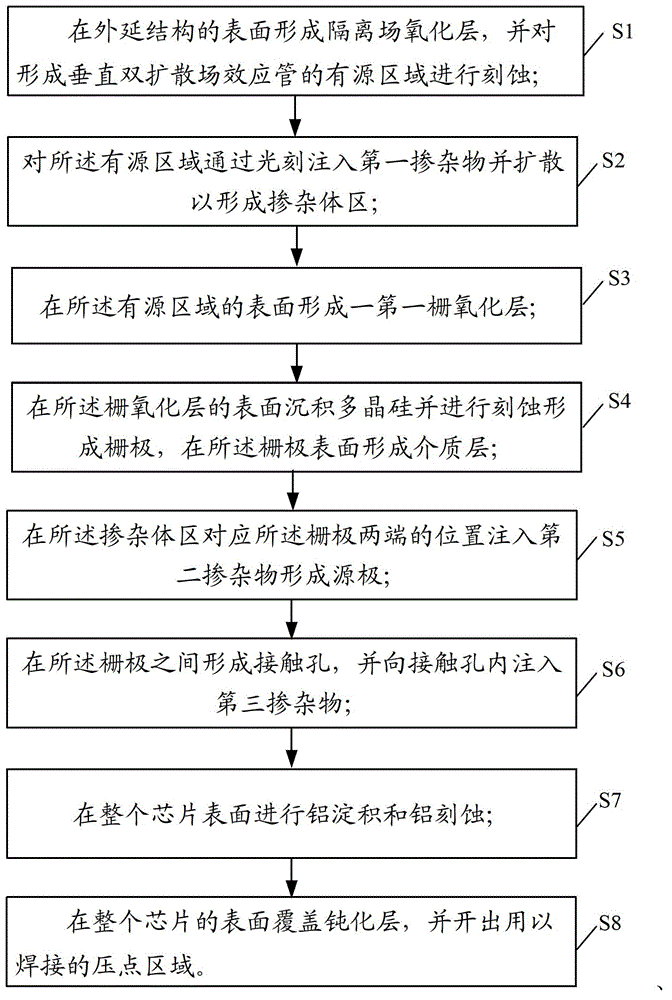
[0036] refer to figure 1 , is shown as a flow chart of the manufacturing process of the vertical double diffused field effect transistor (VDMOS) according to the present invention; its specific steps include the following:

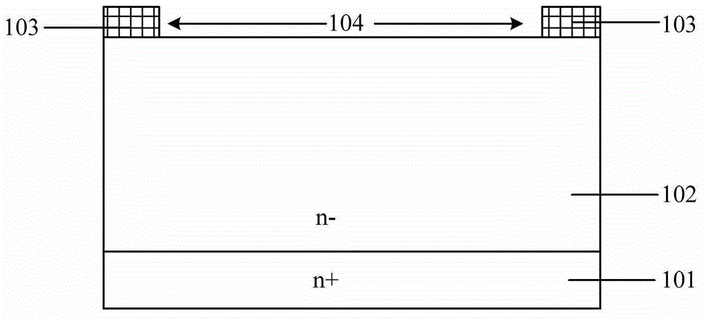
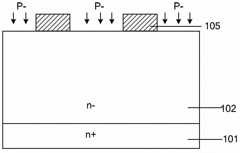
[0037] S1: Form an isolation field oxide layer on the surface of the epitaxial structure, and etch the active regi...


PUM


Abstract

The invention provides a vertical double-diffused field-effect tube and a manufacturing process thereof. In the technical process, after a dopant region is formed, polycrystalline silicon is accumulated to form a grid; and the photoetching frequency is improved, but a photoetching plate is shared for two-time photoetching to reduce production cost. In the manufacturing process for a depletion type vertical double-diffused field-effect tube, the channel injection for the depletion tube is non self-aligned injection, so the breakdown voltage of the vertical double-diffused field-effect tube cannot be reduced, and an electric leakage problem is solved.

Description

technical field [0001] The invention belongs to the field of semiconductor devices, in particular to a vertical double-diffusion field effect transistor and a manufacturing process thereof. Background technique [0002] Vertical double-diffusion MOS (VDMOS) has the advantages of both bipolar transistors and ordinary MOS devices. It has nearly infinite static input impedance characteristics and very fast switching time. Therefore, whether it is a switching application or a linear application, They are all ideal power devices, which can be mainly used in motor speed regulation, inverter, uninterruptible power supply, electronic switch, hi-fi audio, automotive electrical appliances and electronic ballast. However, in the existing vertical double-diffused field-effect transistor manufacturing process, the step of padding polysilicon (Poly) to form the gate is generally set before the formation of the doped body region, so that although only one photolithography is required, the ...

Claims


Application Information

Patent Timeline
IPC IPC(8): H01L21/336H01L29/78
CPCH01L29/0878H01L29/66712H01L29/7802
Inventor 廖忠平
Owner HANGZHOU SILICON-MAGIC SEMICON TECH CO LTD
Why Eureka
Try Eureka