High threshold voltage power mos chip, device and method for increasing threshold voltage
A high-threshold voltage, MOS device technology, applied in the design of MOS devices, the realized MOS devices, and the manufacturing field, can solve the problems of device on-resistance and other parameters increase, device performance degradation, device failure, etc., to achieve a simple threshold voltage , Increase the threshold voltage, the effect of threshold voltage increase
- Summary
- Abstract
- Description
- Claims
- Application Information
AI Technical Summary
Problems solved by technology
Method used
Image

Examples
Embodiment 1
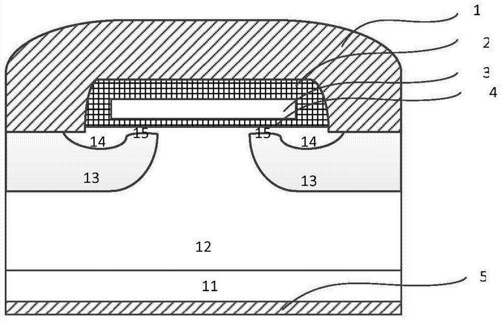
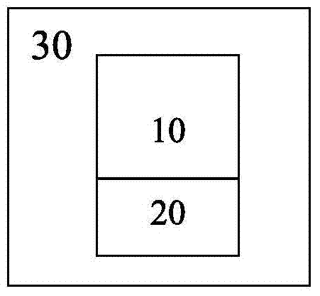
[0056] Figure 4 The circuit schematic diagram of the existing depletion-type N-channel power MOS device is given; in the figure, the depletion-type N-channel MOS device includes a chip, a package body, and pins. The pins include a device source S, a device gate G, and a device drain D; the chip includes an active region 10 (the active region 10 is an active region of a depletion-type N-channel MOS chip), Wire bonding area 30 (including source wire bonding area 31 and polysilicon gate wire bonding area 33); source 1 and polysilicon gate 3 on active area 10 respectively pass through corresponding source wire bonding area 31 and polysilicon gate wire bonding The region 33 is electrically connected to the device source S and the device gate G. The drain 5 is generally a metal layer itself, which is directly electrically connected to the device drain D, and is packaged by the package body 40 to form a depletion-type N-channel. channel MOS devices. Since its specific structure an...
Embodiment 2
[0070] Compared with Embodiment 1, the difference of this embodiment lies mainly in its active region 10, and other parts are similar to Embodiment 1. In order to simplify the description, the following mainly lies in the description of the differences, and only a brief description of other parts. The description is sufficient to enable clear and unambiguous understanding to those of ordinary skill in the art.
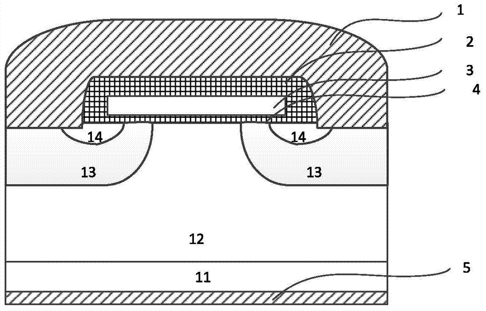
[0071] Figure 7 A schematic circuit diagram of an existing depletion-type P-channel power MOS device is provided; the difference between it and Embodiment 1 is the active region 10 of the depletion-type P-channel power MOS chip in this embodiment , others are similar to Embodiment 1, and the structure and manufacturing process are all prior art, well known to those skilled in the art, and will not be repeated here. Based on this, the present invention makes the following improvements.
[0072] Figure 8 Demonstrated the circuit principle of high threshold voltage d...
Embodiment 3
[0076] Compared with Embodiment 1, the difference of this embodiment lies mainly in its active region 10, and other parts are similar to Embodiment 1. In order to simplify the description, the following mainly lies in the description of the differences, and only a brief description of other parts. The description is sufficient to enable clear and unambiguous understanding to those of ordinary skill in the art.
[0077] Figure 9 A schematic circuit diagram of an existing enhanced N-channel power MOS device is given; the difference from Embodiment 1 is the active region 10 of the enhanced N-channel power MOS chip in this embodiment, Others are similar to Embodiment 1, and the structure and manufacturing process are all prior art and well known to those skilled in the art, and will not be repeated here. Based on this, the present invention makes the following improvements.
[0078] Figure 10 The circuit principle of the high threshold voltage enhanced N-channel power MOS dev...
PUM
 Abstract
Description
Claims
Application Information
 - R&D
- Intellectual Property
- Life Sciences
- Materials
- Tech Scout
- Unparalleled Data Quality
- Higher Quality Content
- 60% Fewer Hallucinations
Browse by: Latest US Patents, China's latest patents, Technical Efficacy Thesaurus, Application Domain, Technology Topic, Popular Technical Reports.
© 2025 PatSnap. All rights reserved.Legal|Privacy policy|Modern Slavery Act Transparency Statement|Sitemap|About US| Contact US: help@patsnap.com