Preparation method of low-conduction voltage drop planar gate IGBT

A planar gate, low conduction technology, applied in semiconductor/solid-state device manufacturing, semiconductor devices, electrical components, etc., can solve the problems of breakdown voltage drop, reverse transmission capacitance increase, etc., and achieve the effect of reducing the conduction voltage drop

Pending Publication Date: 2021-04-13
南瑞联研半导体有限责任公司
View PDF0 Cites 0 Cited by
  • Summary
  • Abstract
  • Description
  • Claims
  • Application Information

AI Technical Summary

Problems solved by technology

[0004] In order to solve the deficiencies of the prior art, the present invention provides a method for preparing a planar gate IGBT with low conduction voltage drop, which can solve the problem of breakdown voltage drop and reverse transmission caused by reducing the conduction voltage drop of the planar gate IGBT in the prior art. The problem of increased capacitance

Method used


Image

  • Preparation method of low-conduction voltage drop planar gate IGBT
  • Preparation method of low-conduction voltage drop planar gate IGBT
  • Preparation method of low-conduction voltage drop planar gate IGBT

Examples


Embodiment Construction

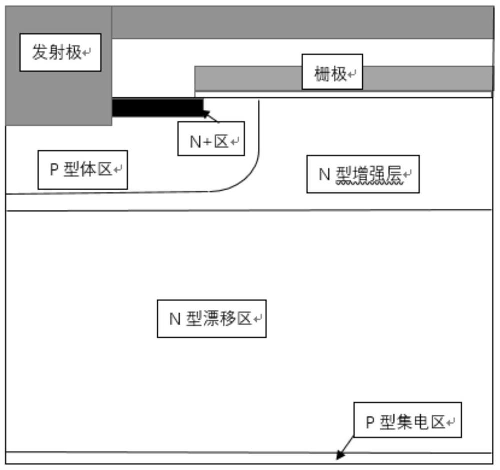
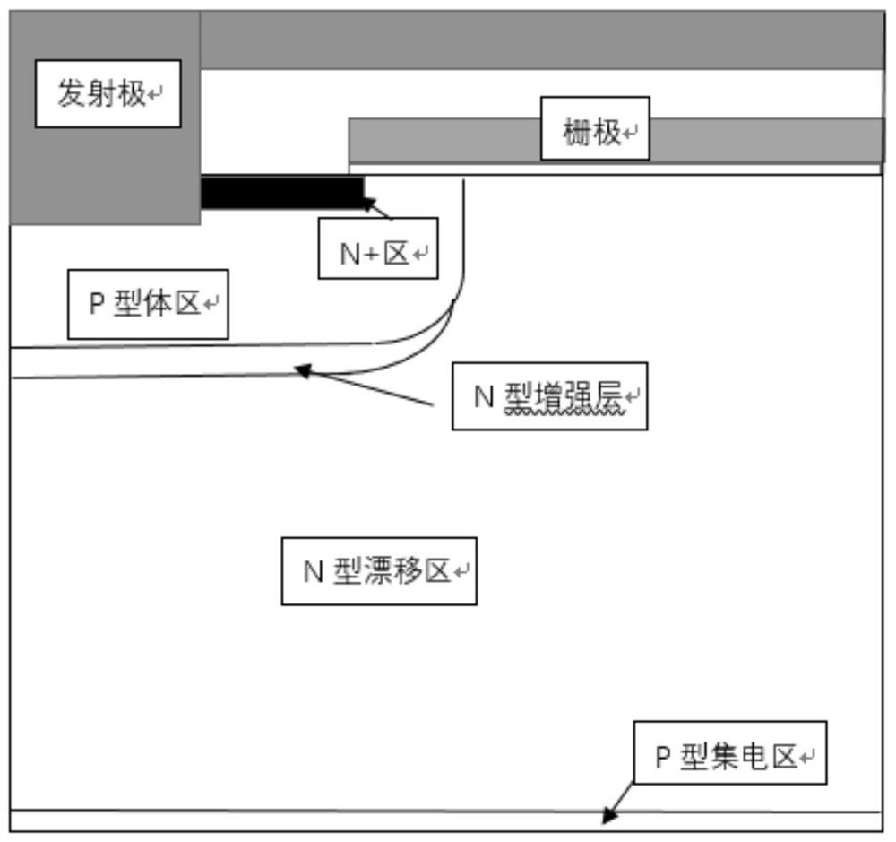
[0038] The present invention will be further described below in combination with embodiments. The following embodiments are only used to illustrate the technical solutions of the present invention more clearly, but not to limit the protection scope of the present invention.

[0039] An embodiment of the present invention provides a method for manufacturing a planar gate IGBT with low conduction voltage drop, including the following steps:

[0040] Step 1: Perform photolithography on the front side of the N-type drift region 1, inject N-type impurities to form a first N-type enhancement part and a second N-type enhancement part in parallel; the second N-type enhancement part is located on the periphery of the first N-type enhancement part, There is a gap between the first N-type enhanced part and the second N-type enhanced part; the implantation depth of the second N-type enhanced part is smaller than that of the first N-type enhanced part.

[0041] The doping concentration of...


PUM


Abstract

The invention belongs to the technical field of power semiconductor device design, and particularly relates to a preparation method of a low-conduction voltage drop planar gate IGBT. The preparation method sequentially prepares an N-type enhancement layer, a P-type body region, an N+ region, a dielectric layer, an emitter, a P-type collector region and a collector, and prepares an N-P-N structure of which the bottom part and the side surface of the P-type body region are N-type enhancement layers, wherein the N-type enhancement layers at the bottom part and the side surface of the P-type body region are not connected. The low-conduction voltage drop planar gate IGBT prepared by the invention has the advantages of high breakdown voltage, low reverse transmission capacitance and relatively low conduction voltage drop.

Description

technical field [0001] The invention belongs to the technical field of power semiconductor device design, and in particular relates to a preparation method of a planar gate IGBT with low conduction voltage drop. Background technique [0002] Compared with trench gate IGBT devices, planar gate IGBT devices have superior reliability, and have been widely used in fields with higher reliability requirements. [0003] In the improved process for planar gate IGBT devices, the commonly used method to reduce the turn-on voltage drop of planar gate IGBT is to inject enhancement type N-type impurities, and the formed N-type enhancement layer is located on the surface of the entire wafer to reduce the IGBT cell-to-cell However, this method will cause the breakdown voltage (BV) of the IGBT to decrease and the reverse transfer capacitance (Cres) to increase. The improved method for this method is to use polycrystalline as a barrier layer after polycrystalline etching, locally inject enh...

Claims


Application Information

Patent Timeline
IPC IPC(8): H01L21/331H01L29/739H01L29/06
CPCH01L29/66333H01L29/7395H01L29/0638
Inventor 高东岳张大华叶枫叶骆健
Owner 南瑞联研半导体有限责任公司
Why Eureka
Try Eureka