Semiconductor device
A semiconductor and transistor technology, applied in the field of semiconductor devices, can solve the problem of high on-resistance and achieve the effect of reducing on-resistance and increasing avalanche tolerance
- Summary
- Abstract
- Description
- Claims
- Application Information
AI Technical Summary
Problems solved by technology
Method used
Image
Examples
no. 1 Embodiment approach )
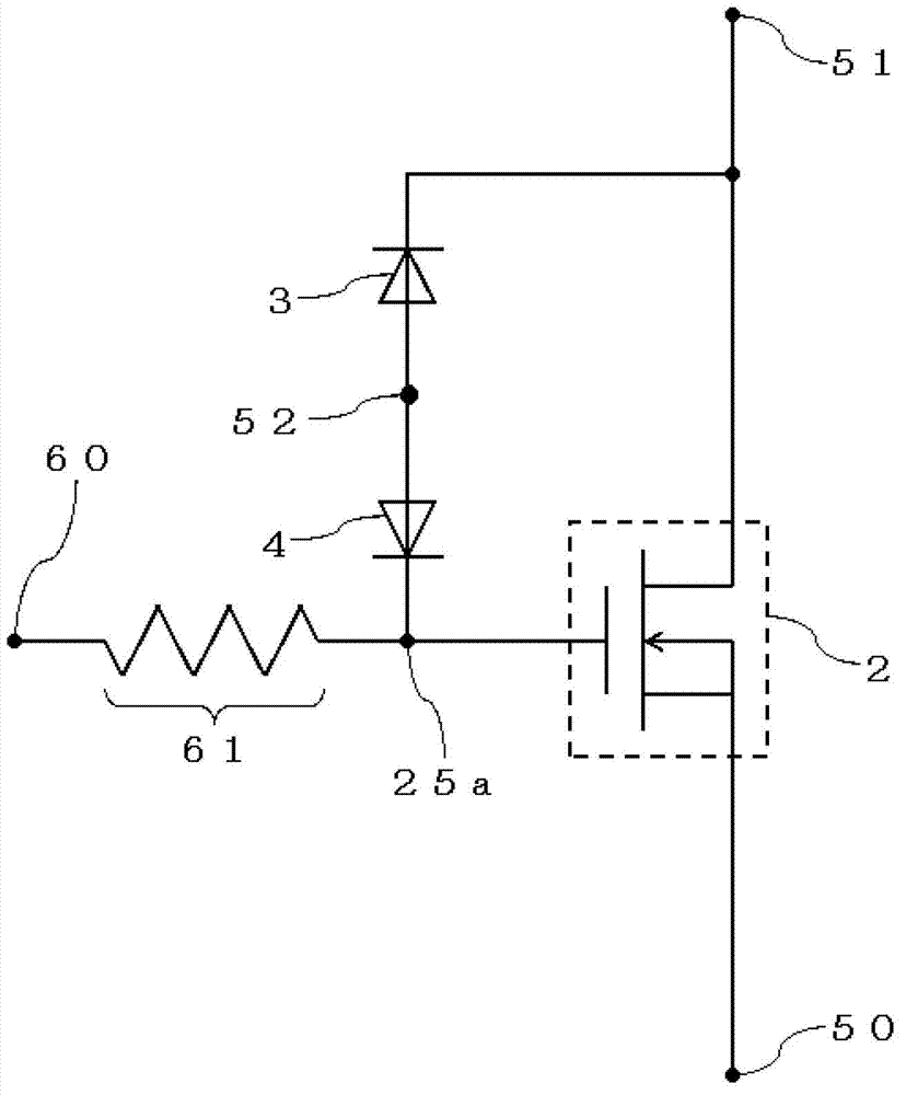
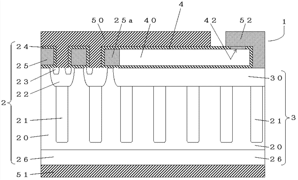
[0027] figure 1 A cross-sectional view showing a main part of the semiconductor device 1 according to the first embodiment is shown, figure 2 An equivalent circuit diagram of the semiconductor device 1 is shown.
[0028] A semiconductor device 1 according to the first embodiment includes a MOS 2 (field effect transistor), a first diode 3 , and a second diode 4 . In addition, this semiconductor device 1 is fabricated by appropriately using both ion implantation and epitaxy on a semiconductor substrate. In this embodiment mode, the semiconductor substrate uses n as the first semiconductor layer - type drift layer 20 is shown. In addition, the plurality of p-type column layers 21 to be the second semiconductor layer are changed from n - One surface side of the drift layer 20 extends in the depth direction and is provided at intervals from each other. As a result, p-type column layer 21 and n - The drift layers 20 are periodically adjacent to each other (pn junctions) to fo...
no. 2 Embodiment approach )
[0048] Figure 4 A cross-sectional view of main parts showing the semiconductor device 1 according to the second embodiment is shown. For each part of the second embodiment, and figure 1 The same parts of the semiconductor device 1 according to the first embodiment shown are denoted by the same reference numerals.
[0049] The semiconductor device 1 of the second embodiment is different from the first embodiment in that a gate electrode 25b leading out the gate electrode 25a is provided on a part of the source electrode 50 provided on the upper portion of the second diode 4, and a The first diode 3 and the second diode 4 are provided.
[0050] The first diode 3 and the second diode 4 are inactive regions where no current flows in the on state of the semiconductor device 1 (MOS 2 ). Generally, the area where the first diode 3 and the second diode 4 are provided is an ineffective area, so as described in this embodiment, by providing the first diode 3 and the second diode 4 o...
no. 3 Embodiment approach )
[0054] Figure 5 A plan view showing main parts of the semiconductor device 1 according to the third embodiment is shown, Image 6 show that Figure 5 The cross-sectional view of the main part of the X‐A‐X' line, Figure 7 A cross-sectional view of a main part of a semiconductor device 1 showing a modified example of the third embodiment is shown. For each part of the third embodiment and the modified example of the third embodiment, and figure 1 The same parts of the semiconductor device 1 according to the first embodiment shown are denoted by the same reference numerals.
[0055] The semiconductor device 1 of the third embodiment is different from the first and second embodiments in that the interval between the p-type clamp layers 30 is set larger than the interval between the p-type base layers 22 . By adopting such a structure, electric field concentration can be generated on the lower end portion of the p-type clamp layer 30 (upper end portion of the p-type column la...
PUM
 Abstract
Description
Claims
Application Information
 - R&D
- Intellectual Property
- Life Sciences
- Materials
- Tech Scout
- Unparalleled Data Quality
- Higher Quality Content
- 60% Fewer Hallucinations
Browse by: Latest US Patents, China's latest patents, Technical Efficacy Thesaurus, Application Domain, Technology Topic, Popular Technical Reports.
© 2025 PatSnap. All rights reserved.Legal|Privacy policy|Modern Slavery Act Transparency Statement|Sitemap|About US| Contact US: help@patsnap.com


