
Insulated gate bipolar transistor (IGBT) device and manufacture process method thereof

A manufacturing process and device technology, which is applied in the field of IGBT devices and its manufacturing process, can solve the problems of expensive equipment, unreachable injection depth, high energy requirement, etc., achieve the optimization of withstand voltage and conduction voltage drop, and improve the safe working area Effect

Active Publication Date: 2013-04-10
SHANGHAI HUAHONG GRACE SEMICON MFG CORP
View PDF7 Cites 8 Cited by
  • Summary
  • Abstract
  • Description
  • Claims
  • Application Information

AI Technical Summary

Problems solved by technology

[0003] For non-penetrating (NPT) IGBTs, in order to achieve high withstand voltage requirements, a thicker N-type base (N base) is required, which increases the conduction voltage drop at the same time, which is not conducive to the use of devices
In order to solve this contradiction, an N-type buffer layer (N buffer) is added between the back P+ collector layer and the N-type base area. Tube annealing is formed, but this technology has three deficiencies. One is that a high-energy ion implanter is required, and the equipment is expensive; the other is that the implantation depth cannot reach more than 2 microns, and the effect of the N-type buffer layer is weakened; The temperature limit behind the metal, the activation efficiency of the N-type buffer layer is not high, which has a certain impact on the device performance

Method used


Image

  • Insulated gate bipolar transistor (IGBT) device and manufacture process method thereof
  • Insulated gate bipolar transistor (IGBT) device and manufacture process method thereof
  • Insulated gate bipolar transistor (IGBT) device and manufacture process method thereof

Examples


Embodiment Construction

[0056]In order to enable your examiners to have a further understanding and understanding of the purpose, features and effects of the present invention, the following detailed description is as follows with the accompanying drawings.

[0057] The steps of the first embodiment of the method of the present invention include:

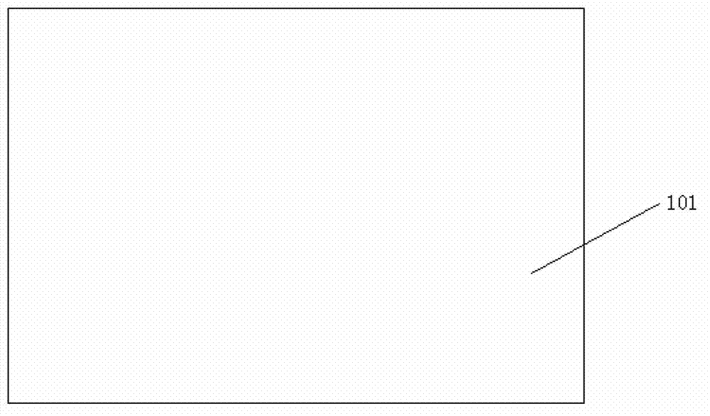
[0058] Step 1. Prepare an N-type region of molten silicon as the N-base region 101, such as Figure 1a shown. The thickness of the molten silicon in the N-type region may be 725 microns.

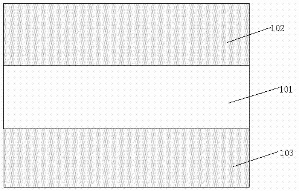
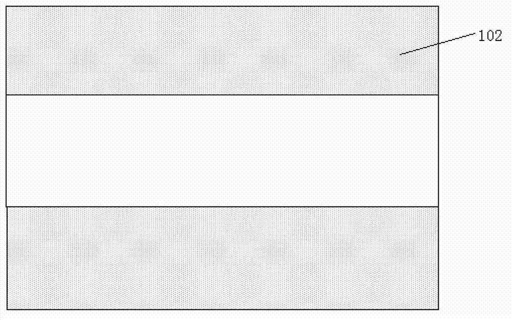
[0059] Step 2. Perform double-sided high-temperature N-type impurity diffusion on the N-base region 101. A high-temperature phosphorus doping process (POCL3 process) can be used to form a certain depth of double-sided N-type doped regions, including the front N-type doped region 102 and N-type doped region 103 on the back; as Figure 1b shown. The depth of one side is usually 90-110 microns for 3300V IGBT; 50-70 microns for 4500V IGBT; 10-30 microns for 6500VIGBT.

...


PUM


Abstract

The invention discloses a manufacture process method for an insulated gate bipolar transistor (IGBT). Double-sided N type impurity diffusion is carried out on an N base zone to form a double-sided N type mixed zone which comprises a front N type mixed zone and a back N type mixed zone. The front N type mixed zone is thinned, and the remained front N type zone serves as a carrier storage layer. The back N type mixed zone is thinned, and the remained back N type zone serves as an N type buffer layer. Thus, a front carrier storage layer is formed to improve a safe working zone of the device. Simultaneously, the deep N type buffer layer is formed at the back to furthest optimize voltage resistance and drop voltage of a device. The invention simultaneously discloses a device manufactured with the method.

Description

technical field [0001] The invention relates to a manufacturing process method of a semiconductor integrated circuit, in particular to a manufacturing process method of an IGBT device; the invention also relates to a device manufactured by the method. Background technique [0002] IGBT (Insulated Gate Bipolar Transistor), based on the power field effect transistor (VDMOS), adds a thin layer of P+ under the drift region (N-layer of N-type IGBT) that withstands high voltage, and introduces a conductive The modulation effect greatly improves the current handling capability of the device, but at the same time, the introduction of the P+ thin layer makes the IGBT have one more PNP transistor than the power field effect transistor, which is easy to cause latch-up and reduce the safe operating area. For this reason, a carrier storage layer (CS layer) is added under the p-well region (P-well), which improves the anti-latch-up capability of the IGBT. The general technique to realize...

Claims


Application Information

Patent Timeline
Patent Type & Authority Applications(China)
IPC IPC(8): H01L21/331H01L29/06H01L29/739
Inventor 李娜
Owner SHANGHAI HUAHONG GRACE SEMICON MFG CORP
Learn More