Deposition method of Cu/ZnO/Al photoelectric transparent conducting film
A technology of transparent conductive film and deposition method, which is applied in the direction of circuits, electrical components, semiconductor devices, etc., can solve the problems of high hardness of FTO film, high preparation process requirements, doping process and other problems, and achieve easy control of the deposition process and excellent photoelectric performance. Excellent, simple preparation process
- Summary
- Abstract
- Description
- Claims
- Application Information
AI Technical Summary
Problems solved by technology
Method used
Image

Examples
Embodiment 1
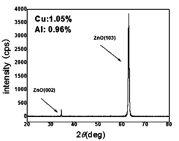
[0027] After the substrate was cleaned with acetone, ethanol and deionized water by ultrasonic waves in sequence, it was blown dry with nitrogen and sent to the reaction chamber.
[0028] Vacuum the background of magnetron sputtering to 9.0×10 -4 After pa, the substrate is heated to 100°C and the gas flow rate is adjusted to make the pressure reach 5Pa, the sputtering power is 100W, the sputtering time is 1min, and the thickness of the Al film is 30nm.
[0029] Then, the ZnO film was deposited and prepared by plasma-enhanced electron cyclotron resonance chemical vapor deposition, and the vacuum was pumped to 7.0×10 -4 After Pa, the substrate was heated to 100°C, and diethylzinc Zn(CH 2 CH 3 ) 2 and oxygen O 2 After that, Zn(CH 2 CH 3 ) 2 and O 2 The flow ratio is controlled by a mass flow meter to be 1sccm:100sccm, and the total pressure of the gas is controlled to be 1.6Pa; at the electron cyclotron resonance frequency of 650Hz, the reaction takes 25min to obtain a 40...
Embodiment 2
[0037] After cleaning the substrate with acetone, ethanol and deionized water with ultrasonic waves in sequence, blow it dry with nitrogen and send it into the reaction chamber, and vacuum the background of magnetron sputtering to 9.0×10 -4 After pa, the substrate is heated to 100°C and the gas flow rate is adjusted so that the pressure reaches 5Pa, the sputtering power is 100W, and the sputtering time is 1min. The Al film has a film thickness of 30nm.
[0038] Then, the ZnO film was deposited and prepared by plasma-enhanced electron cyclotron resonance chemical vapor deposition, and the vacuum was pumped to 7.0×10 -4 After Pa, the substrate was heated to 100°C, and diethylzinc Zn(CH 2 CH 3 ) 2 and oxygen O 2 After that, Zn(CH 2 CH 3 ) 2 and O 2 The amount is controlled by a mass flow meter to 2sccm: 200sccm, and the total pressure of the controlled gas is 1.8Pa; at the electron cyclotron resonance frequency of 650Hz, react for 30 minutes to obtain a 500nm ZnO thin film...
Embodiment 3
[0045] After cleaning the substrate with acetone, ethanol and deionized water with ultrasonic waves in sequence, blow it dry with nitrogen and send it into the reaction chamber, and vacuum the background of magnetron sputtering to 9.0×10 -4 After pa, the substrate is heated to 100° C. and the gas flow rate is adjusted to make the air pressure reach 5 Pa, the sputtering power is 100 W, and the sputtering time is 5 min for an Al thin film with a film thickness of 50 nm.
[0046] Then, the ZnO film was deposited and prepared by plasma-enhanced electron cyclotron resonance chemical vapor deposition, and the vacuum was pumped to 7.0×10 -4 After Pa, the substrate was heated to 100°C, and diethylzinc Zn(CH 2 CH 3 ) 2 and oxygen O 2 After that, Zn(CH 2 CH 3 ) 2 and O 2 The amount is controlled by a mass flow meter to 2sccm: 150sccm, and the total pressure of the controlled gas is 2.0Pa; at the electron cyclotron resonance frequency of 650Hz, react for 40min to obtain a 600nm Zn...
PUM
| Property | Measurement | Unit |
|---|---|---|
| thickness | aaaaa | aaaaa |
| thickness | aaaaa | aaaaa |
| electrical resistivity | aaaaa | aaaaa |
Abstract
Description
Claims
Application Information
 - Generate Ideas
- Intellectual Property
- Life Sciences
- Materials
- Tech Scout
- Unparalleled Data Quality
- Higher Quality Content
- 60% Fewer Hallucinations
Browse by: Latest US Patents, China's latest patents, Technical Efficacy Thesaurus, Application Domain, Technology Topic, Popular Technical Reports.
© 2025 PatSnap. All rights reserved.Legal|Privacy policy|Modern Slavery Act Transparency Statement|Sitemap|About US| Contact US: help@patsnap.com