Method for preparing silicon-based nano-scale ordered porous silicon
A nano-sized, porous silicon technology, applied in the field of silicon-based porous silicon, can solve the problem that porous silicon cannot satisfy high specific surface area and highly ordered pores at the same time, and achieve excellent performance, highly ordered pores, and large specific surface area Effect
- Summary
- Abstract
- Description
- Claims
- Application Information
AI Technical Summary
Problems solved by technology
Method used
Image
Examples
Embodiment 1
[0027] (1) Wafer cleaning:
[0028] An n-type (100) single-sided polished single-crystal silicon wafer with a resistivity of 0.015Ω·cm and a thickness of 400±10μm is cut into a rectangular silicon substrate with a size of 2.2cm×0.8cm, and put into acetone solvent in turn, Ultrasonic cleaning in absolute ethanol and deionized water for 20 minutes respectively, followed by soaking in 5% hydrofluoric acid aqueous solution for 15 minutes, and then washing with deionized water for later use.
[0029] (2) Preparation of silicon-based porous silicon:
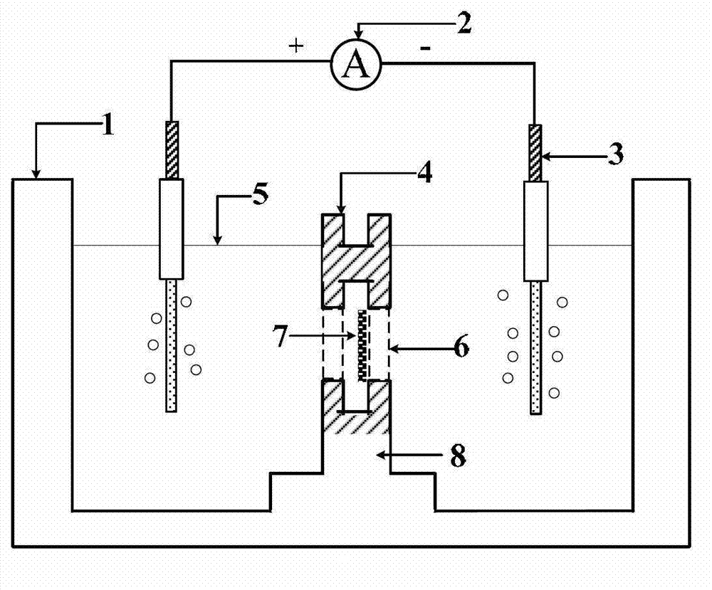
[0030] A porous silicon layer was prepared on the polished surface of a silicon wafer by a double-groove electrochemical etching method. Firstly, the hydrofluoric acid aqueous solution with a mass fraction of 7% is added into the electrochemical corrosion tank as a corrosion solution, without adding surfactants and oxidants; then a pair of platinum metal electrodes are respectively inserted into the two half tanks as cathode and anode...
Embodiment 2
[0033] This embodiment is similar to Embodiment 1, except that the corrosion solution used in step (2) is a hydrofluoric acid aqueous solution with a mass fraction of 6%, and the applied corrosion current density is 120mA / cm 2 , the corrosion time is 20min. The scanning electron microscope photos of the prepared silicon-based porous silicon surface morphology and cross-sectional structure are as follows: Figure 4 and Figure 5 shown. The average pore diameter of the prepared porous silicon parameters is 227.81nm, the layer thickness is 33.39μm, and the porosity is 66%. The hole wall is relatively smooth.
Embodiment 3
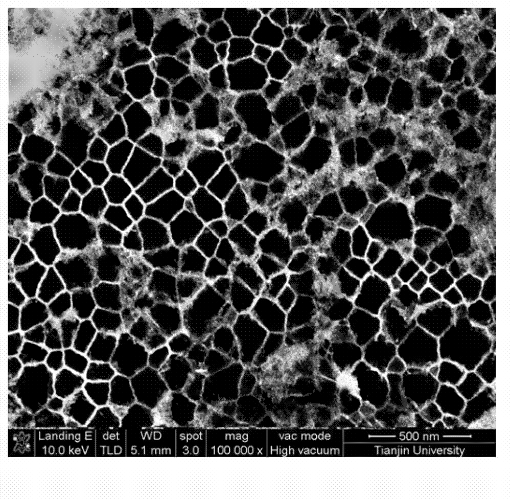
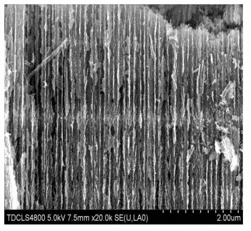
[0035] This embodiment is similar to Embodiment 1, except that the corrosion solution used in step (2) is a hydrofluoric acid aqueous solution with a mass fraction of 7%, and the applied corrosion current density is 125mA / cm 2 , the corrosion time is 15min. The scanning electron microscope photos of the prepared silicon-based porous silicon surface morphology and cross-sectional structure are as follows: Figure 6 and Figure 7 As shown, the average pore diameter of the prepared porous silicon parameters is 112.25nm, the layer thickness is 53.42μm, the porosity is 68.75%, the surface morphology is a honeycomb structure composed of polygonal pores, and the cross-sectional morphology is straight cylindrical. sequence, the walls of the pores are very rough and side pores appear.
[0036] In the present invention, the method of weighing samples with an electronic balance is adopted, and the porosity and thickness of silicon-based porous silicon are obtained through formula calcu...
PUM
| Property | Measurement | Unit |
|---|---|---|
| electrical resistivity | aaaaa | aaaaa |
| thickness | aaaaa | aaaaa |
| pore size | aaaaa | aaaaa |
Abstract
Description
Claims
Application Information
 - R&D
- Intellectual Property
- Life Sciences
- Materials
- Tech Scout
- Unparalleled Data Quality
- Higher Quality Content
- 60% Fewer Hallucinations
Browse by: Latest US Patents, China's latest patents, Technical Efficacy Thesaurus, Application Domain, Technology Topic, Popular Technical Reports.
© 2025 PatSnap. All rights reserved.Legal|Privacy policy|Modern Slavery Act Transparency Statement|Sitemap|About US| Contact US: help@patsnap.com


