Double-emitting layer hemispherical shell-shaped organic electroluminescent device and its preparation method
A hemispherical shell, dual emission technology, applied in semiconductor/solid-state device manufacturing, semiconductor devices, electric solid-state devices, etc., can solve the problems of annihilation and hinder the application of phosphorescent OLED devices, reduce the starting voltage, widen the collision recombination area, reduce the Annihilation effect
- Summary
- Abstract
- Description
- Claims
- Application Information
AI Technical Summary
Problems solved by technology
Method used
Image
Examples
preparation example Construction
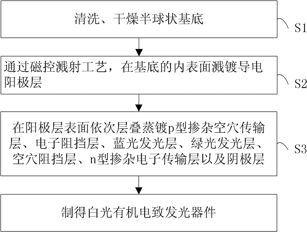
[0047] The preparation method of the above-mentioned double-emitting layer hemispherical shell-shaped organic electroluminescent device, such as figure 2 shown, including the following steps:
[0048] S1. The hemispherical substrate (eg, glass) is ultrasonically cleaned with purified water, acetone, ethanol, etc. for 15 minutes in sequence, and dried after cleaning;
[0049] S2. Using a magnetron sputtering process, the hemispherical shell-shaped substrate is placed in a vacuum chamber of a magnetron sputtering device, and an anode layer is sputtered on the inner surface of the hemispherical shell-shaped substrate; the hemispherical shell-shaped anode substrate is obtained, Subsequently, the anode layer was treated with oxygen plasma with a power of 10W for 15min;
[0050] S3. Put the hemispherical shell-shaped anode substrate into the organic vacuum chamber of the evaporation equipment, and sequentially evaporate the p-type doped hole transport layer, light-emitting layer, ...
Embodiment 1
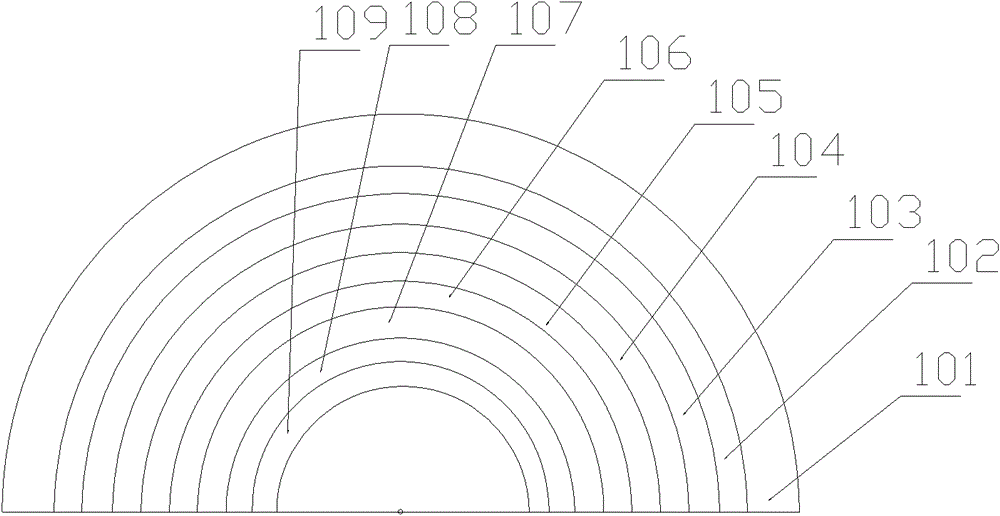
[0056] The structure of the hemispherical organic electroluminescence device of the present embodiment is: glass / ITO / m-MTDATA:F4-TCNQ / TAPC / (TCTA:TPBi):Firpic:Ir(MDQ) 2 (acac) / (TCTA:TPBi):Ir(ppy) 3 :Ir(MDQ) 2 (acac) / Bphen / Bphen:Cs 2 CO 3 / Mg:Ag.
[0057] The preparation steps of the hemispherical shell-shaped organic electroluminescent device with double emission layers in this embodiment are as follows:
[0058] 1. Clean the hemispherical glass substrate with an inner diameter of 5mm and a thickness of 2mm with pure water, acetone, ethanol, etc. for 15 minutes, and then dry it;
[0059] 2. Put the hemispherical glass substrate into the organic vacuum chamber of the magnetron sputtering equipment, sputter a layer of 150nm thick ITO anode layer; then spin-coat the glass coated with the ITO anode layer with photoresist, expose and develop , Aqua regia etching, etch into the required pattern and size, then clean the etched conductive glass, and then use pure water, acetone, e...
Embodiment 2
[0064] The structure of the hemispherical shell-shaped organic electroluminescent device with double emission layers of the present embodiment is:
[0065] Glass / FTO / TPD:TCNQ / TPD / (TCTA:TPBi):FIr6:Ir(MDQ) 2 (acac) / (TCTA:TPBi):Ir(ppy) 3 :Ir(MDQ) 2 (acac) / PBD / PBD:LiF / Ag.
[0066] The preparation steps of the hemispherical shell-shaped organic electroluminescent device with double emission layers in this embodiment are as follows:
[0067] 1. The hemispherical glass substrate with an inner diameter of 5 mm and a thickness of 4 mm was ultrasonically cleaned with purified water, acetone, ethanol, etc. for 15 minutes, cleaned and dried;
[0068] 2. Put the hemispherical glass substrate into the organic vacuum chamber of the magnetron sputtering equipment, sputter a layer of FTO anode layer with a thickness of 180nm; then spin-coat the glass coated with the FTO anode layer with photoresist, expose and develop , Aqua regia etching, etch into the required pattern and size, then clea...
PUM
| Property | Measurement | Unit |
|---|---|---|
| thickness | aaaaa | aaaaa |
| thickness | aaaaa | aaaaa |
| thickness | aaaaa | aaaaa |
Abstract
Description
Claims
Application Information
 - R&D
- Intellectual Property
- Life Sciences
- Materials
- Tech Scout
- Unparalleled Data Quality
- Higher Quality Content
- 60% Fewer Hallucinations
Browse by: Latest US Patents, China's latest patents, Technical Efficacy Thesaurus, Application Domain, Technology Topic, Popular Technical Reports.
© 2025 PatSnap. All rights reserved.Legal|Privacy policy|Modern Slavery Act Transparency Statement|Sitemap|About US| Contact US: help@patsnap.com


