High-precision integrated circuit device testing equipment

A technology for integrated circuits and test equipment, applied in the field of test equipment, can solve the problems of low test accuracy, complex test structure, large occupied area, etc., and achieve the effects of suppressing the influence of leakage current, reducing the influence of parasitic parameters, and simple instrument structure

Active Publication Date: 2016-03-30
INST OF MICROELECTRONICS CHINESE ACAD OF SCI
View PDF4 Cites 0 Cited by
  • Summary
  • Abstract
  • Description
  • Claims
  • Application Information

AI Technical Summary

Problems solved by technology

However, for the MOS structure of new nano-devices, the EOT is usually less than 1.4nm, the leakage current is greater than 0.1pA, and the minimum gate capacitance and channel capacitance to be tested are less than 1pF
Therefore, the serious leakage (Leakage>0.1pA) of the ultra-thin gate dielectric (EOT<1.4nm) affects the test accuracy of the equivalent impedance
[0006] In addition, due to the difficulty of direct testing of ultra-small channel capacitance, special device test structures are usually required. Three methods for measuring tiny capacitance, such as charge injection method, AC excitation method and AC excitation method with balanced capacitance, all need to be tested on the wafer. Make hundreds of series and parallel transistors (that is, measure the stray capacitance or distributed capacitance of the circuit) to increase the equivalent capacitance of the test, and then calculate the actual measurement through the test circuit of feedback impedance, pre-operational amplifier, multiplier, etc. MOS capacitance, but this will affect the effective area of ​​the chip. In addition, the parasitic impedance in these test circuits and the fluctuation of the excitation signal source will also seriously affect the accuracy of the test.
[0007] All in all, the existing methods and equipment for measuring the tiny capacitance of MOS devices are no longer suitable for small-sized devices, especially nanometer devices, with low test accuracy and complex test structures, which occupy a large area

Method used


Image

  • High-precision integrated circuit device testing equipment
  • High-precision integrated circuit device testing equipment
  • High-precision integrated circuit device testing equipment

Examples


Embodiment Construction

[0023] The features and technical effects of the technical solution of the present invention will be described in detail below with reference to the accompanying drawings and in combination with schematic embodiments, and a device for testing the capacitance of a nanometer device channel ultra-thin gate dielectric is disclosed. It should be pointed out that similar reference numerals represent similar structures, and the terms "first", "second", "upper", "lower" and the like used in this application can be used to modify various device structures or process steps . These modifications do not imply spatial, sequential or hierarchical relationships of the modified device structures or process steps unless otherwise specified.

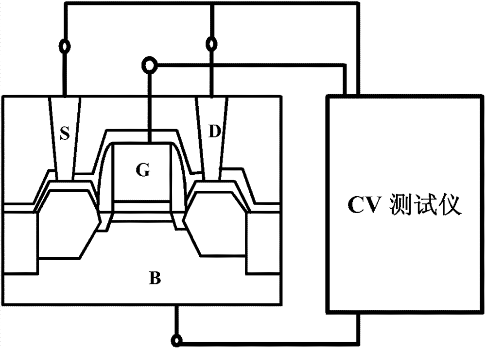
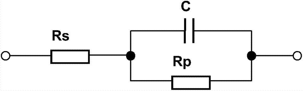
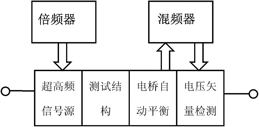
[0024] refer to figure 1 , shows a schematic diagram of a test structure for indirectly measuring effective mobility by measuring MOS capacitance according to the present invention. Using the RF-UHF dual-frequency capacitance testing instrument describe...


PUM


Abstract

The invention provides testing equipment for piece capacitance of a high-precise integrated circuit device, comprising a frequency multiplier, a high-frequency signal source, a bridge automatic balancing module, a frequency mixer and a voltage vector detection module, wherein base frequency signals are multiplied to the high frequency by the frequency multiplier; the testing signals are transmitted to a device to be tested by the high-frequency signal source; the output testing result signals are transmitted to the frequency mixer by the bridge automatic balancing module so as to reduce the base frequency; and then the output testing result signals output the final testing result through the a voltage vector detection module; the testing equipment is characterized in that the high-frequency signal source generates high-frequency testing signals with different frequencies (ultra-high frequency band ranges from 2 to 200MHz, and radio frequency is greater than 1 GHz) by the frequency multiplier so as to be used for the equivalent impedance test for the tested capacitance. The testing equipment for the piece capacitance of the high-precise integrated circuit device can test the equivalent impedance and piece capacitance of the nano integrated circuit device precisely; the equipment is simple in structure; the radio frequency test can restrain the capacity fall-off influence; the double-frequency test reduces the influence of stray parameters; and a complex testing instrument, such as a network analyzer as well as a special testing structure are not needed.

Description

technical field [0001] The invention relates to a testing device, in particular to a testing device for on-chip capacitance or equivalent impedance of a high-precision integrated circuit device. Background technique [0002] Starting from the 90nm CMOS integrated circuit technology node, with the continuous reduction of device feature size, a number of new integrated circuit technologies, new materials and new processes have been continuously introduced into the device structure to continuously improve device and circuit performance. These new technologies include channel strain, high mobility channel (Ge, III-V) heterogeneous integration, etc. [0003] These new nano-MOS device structures can effectively overcome short-channel effects, parasitic effects, and improve electrical conductivity, etc., but the size and material composition of each part of the device structure can affect the final device performance. The practical impact of nanochannel transport properties (such ...

Claims


Application Information

Patent Timeline
Patent Type & Authority Patents(China)
IPC IPC(8): G01R31/28G01R27/26G01R27/08
Inventor 殷华湘梁擎擎钟汇才
Owner INST OF MICROELECTRONICS CHINESE ACAD OF SCI
Why Eureka
Try Eureka