Self-assembling growth method of compound semiconductor film
A growth method and semiconductor technology, applied in the fields of semiconductor/solid-state device manufacturing, electrical components, circuits, etc., can solve the problems of insufficient nucleation density and dislocation density, improve device performance, reduce dislocation and dislocation density, etc. reduced effect
- Summary
- Abstract
- Description
- Claims
- Application Information
AI Technical Summary
Problems solved by technology
Method used
Image
Examples
Embodiment 1
[0030] Embodiment 1: A self-assembled growth method of gallium nitride semiconductor thin film.
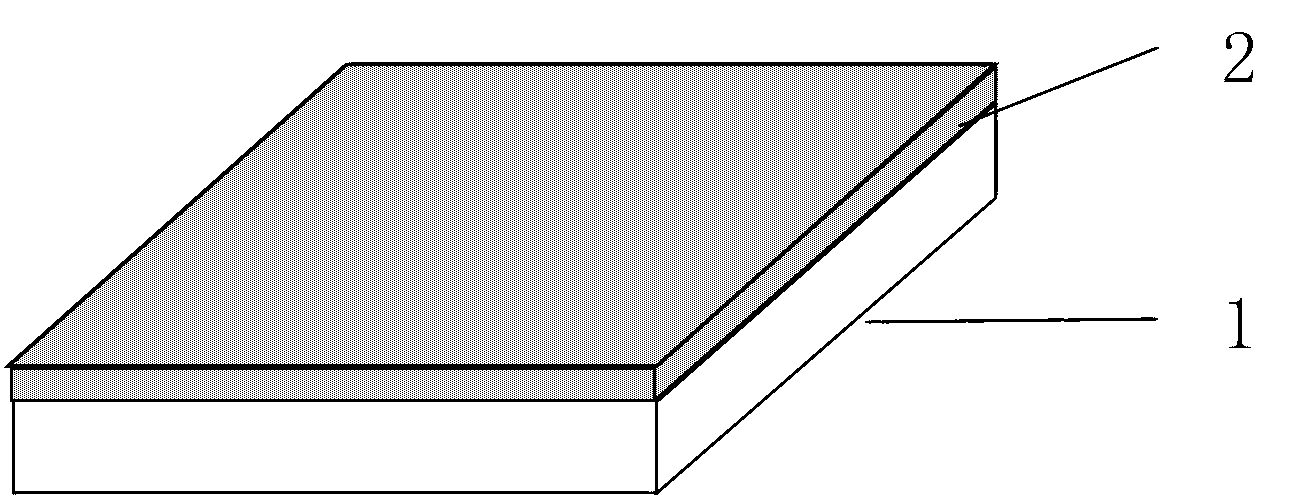
[0031] Step 1: The temperature of the MOCVD reaction chamber is raised to 500°C, the pressure is 600~650mbar, and trimethylgallium is introduced for 3 minutes, and a decomposition reaction occurs on the sapphire (0001) substrate to form a 10nm metal thin layer.
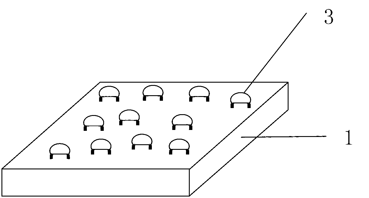
[0032] Step 2: Raise the temperature to 900°C and reduce the pressure to 500~550mbar, the metal condenses into small balls with a density of 2.3×10 6 cm -2 , the diameter of the pellet is 400-600nm, and the duty cycle is 65%.
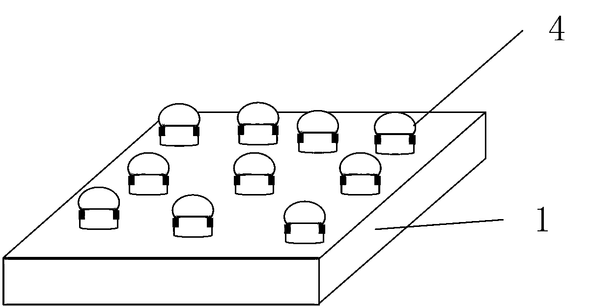
[0033] Step 3: Keep the temperature at 900°C and the pressure at 500-550mbar, and inject hydrogen, trimethylgallium and ammonia gas, and the gallium nitride crystal nuclei are formed at the bottom of the gold particles, with a diameter of 500-800nm.
[0034] Step 4: Increase the temperature to 1000 o C, injecting hydrogen, trimethylgallium and ammonia gas, wherein the V / III ratio is 50, the pres...
Embodiment 2
[0037] Embodiment 2: A self-assembly growth method of an indium nitride semiconductor thin film.
[0038] Step 1: The temperature of the MOCVD reaction chamber is raised to 350°C, the pressure is 600mbar, and trimethyl indium is passed through for 3 minutes, and a decomposition reaction occurs on the sapphire (0001) substrate to form a 10nm metal thin layer.
[0039] Step 2: After 3 minutes, the temperature is raised to 450°C, the pressure is reduced to 500mbar, and the metal condenses into small balls with a density of 1.2×10 6 cm -2 , the diameter of the pellet is 400-600nm, and the duty cycle is 60%.
[0040] Step 3: Keep the temperature at 450° C. and the pressure at 500 mbar, and inject hydrogen, trimethylindium and ammonia gas for 2 minutes. Indium nitride nuclei are formed at the bottom of the gold particles, with a diameter of 400-600 nm.
[0041] Step 4: Increase the temperature to 500 o C, Introduce hydrogen, trimethylindium and ammonia for 20 minutes, wherein the...
Embodiment 3
[0044] Embodiment 3: A self-assembly growth method of an aluminum nitride semiconductor thin film.
[0045] Step 1: The temperature of the MOCVD reaction chamber is raised to 600°C, the pressure is 600mbar, and trimethylaluminum is introduced for 5 minutes, and a decomposition reaction occurs on the sapphire (0001) substrate to form a 15nm metal thin layer.
[0046] Step 2: Raise the temperature to 1150°C and lower the pressure to 500mbar, the metal condenses into small balls with a density of 5.0×10 6 cm -2 , the diameter of the ball is 400-600nm, and the duty cycle is 70%.
[0047] Step 3: Keep the temperature at 1150° C. and the pressure at 500 mbar, inject hydrogen, trimethylaluminum and ammonia, and form gallium nitride nuclei at the bottom of the gold particles, with a diameter of 500-800 nm.
[0048] Step 4: Increase the temperature to 800 o C, injecting hydrogen, trimethylaluminum and ammonia gas, wherein the V / III ratio is 200, the pressure is maintained at 500mbar...
PUM
| Property | Measurement | Unit |
|---|---|---|
| Diameter | aaaaa | aaaaa |
| Height | aaaaa | aaaaa |
| Diameter | aaaaa | aaaaa |
Abstract
Description
Claims
Application Information
 - R&D Engineer
- R&D Manager
- IP Professional
- Industry Leading Data Capabilities
- Powerful AI technology
- Patent DNA Extraction
Browse by: Latest US Patents, China's latest patents, Technical Efficacy Thesaurus, Application Domain, Technology Topic, Popular Technical Reports.
© 2024 PatSnap. All rights reserved.Legal|Privacy policy|Modern Slavery Act Transparency Statement|Sitemap|About US| Contact US: help@patsnap.com


