Antimony-rich high-speed phase change material for phase change memory, method for preparing antimony-rich high-speed phase change material and application of material
A technology of phase-change memory and phase-change materials, which is applied in the field of antimony-rich high-speed phase-change materials and their preparation, can solve the problems of low crystallization temperature and cannot fully meet the needs of applications, and achieve mature preparation technology, stable resistance, and small volume effect of change
- Summary
- Abstract
- Description
- Claims
- Application Information
AI Technical Summary
Problems solved by technology
Method used
Image
Examples
Embodiment 1
[0039] 1. Using magnetron sputtering W and Sb 2 Preparation of W on thermally oxidized silicon substrates by Te double-target co-sputtering x (Sb 2 Te) 1-x Thin films, when co-sputtering, the background vacuum is 2.0×10 -4 Pa, the argon gas pressure during sputtering is 0.22Pa. Sb 2 The sputtering power of the Te target is locked at radio frequency (RF) 20W, and the sputtering power of the W target is changed to radio frequency (RF) 0W, 5W, 7W, 10W respectively, and four kinds of phase change films a#, b#, c#, d#. The parameters of the four thin film phase change materials are shown in Table 1 below:
[0040] Table 1
[0041]
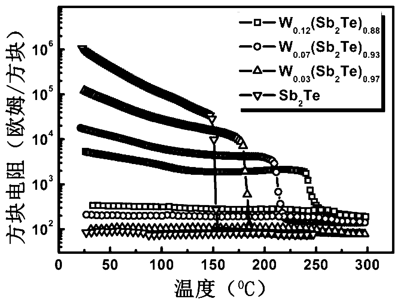
[0042] 2. W x (Sb 2 Te) 1-x Thin film materials were tested for in-situ resistance, and the results were as follows: figure 1 shown. It can be seen that the Sb without W doping 2 Te crystallization temperature is 145°C. After the addition of W element, the crystallization temperature of the phase change film is greatly improved, and the...
Embodiment 2
[0048] 1. Preparation of Ti on thermally oxidized silicon substrates by magnetron sputtering 0.1 (Sb 2 Te) 0.9 film. The specific experimental method is: use the prepared Ti 0.1 (Sb 2 Te) 0.9 Single target sputtering, the power is RF 30W, the background vacuum is 1.8×10 -4 Pa, the argon gas pressure during sputtering is 0.19Pa, and the film thickness is 200nm.
[0049] 2. Testing Ti with in-situ resistance-temperature 0.1 (Sb 2 Te) 0.9 The crystallization temperature of the film is 225°C, and the data retention is calculated to be 137°C, both values are much higher than Ge 2 Sb 2 Te 5 film.
[0050] 3. Ti 0.1 (Sb 2 Te) 0.9 The volume change before and after the phase transition of the thin film is very small, the grain distribution is very uniform, and there is no phase separation, which is very suitable for high-speed and high-density memory.
PUM
| Property | Measurement | Unit |
|---|---|---|
| melting point | aaaaa | aaaaa |
| crystallization temperature | aaaaa | aaaaa |
Abstract
Description
Claims
Application Information
 - R&D
- Intellectual Property
- Life Sciences
- Materials
- Tech Scout
- Unparalleled Data Quality
- Higher Quality Content
- 60% Fewer Hallucinations
Browse by: Latest US Patents, China's latest patents, Technical Efficacy Thesaurus, Application Domain, Technology Topic, Popular Technical Reports.
© 2025 PatSnap. All rights reserved.Legal|Privacy policy|Modern Slavery Act Transparency Statement|Sitemap|About US| Contact US: help@patsnap.com


