Output buffer

A technology of output buffer and output terminal, applied in the direction of logic circuit connection/interface layout, etc., can solve the problems of large output jitter of output signal OUT, unfavorable noise, large signal delay time, etc.

Inactive Publication Date: 2015-02-25
NOVATEK MICROELECTRONICS CORP
View PDF7 Cites 0 Cited by
  • Summary
  • Abstract
  • Description
  • Claims
  • Application Information

AI Technical Summary

Problems solved by technology

Under the trend of reducing the power supply voltage level of the output stage, the driving current of the high-voltage transistor will be weakened accordingly, resulting in a large signal delay time
At the same time, the low operating voltage is relatively unfavorable against the noise generated during synchronous operation from the power supply
As a result, the output signal OUT will have a large output jitter

Method used


Image

  • Output buffer
  • Output buffer

Examples


Embodiment Construction

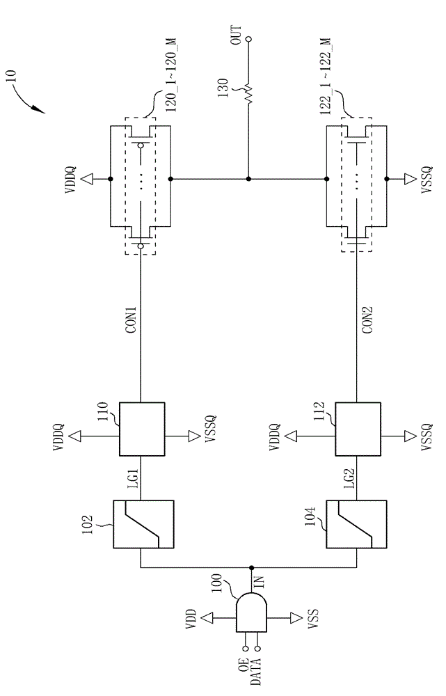
[0052]The output buffer provided in the following embodiments can maintain the stability of the output signal when the operating voltage keeps dropping. The following embodiments consider that in the Complementary Metal-Oxide-Semiconductor (CMOS) process, the driving current of the low-voltage transistor is weakened by the reduction of the supply voltage level is less obvious, so the output buffer Some components in the converter that are not directly facing the load are implemented with low-voltage components. As a result, the output buffer has better resistance to power supply noise, and can achieve a smaller delay time of the output signal, thereby making it easier to achieve a low-jitter output signal.

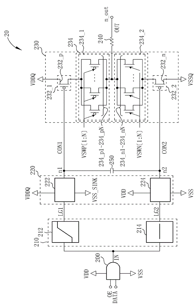
[0053] Please refer to figure 2 , figure 2 It is a schematic structural diagram of an output buffer 20 according to an embodiment. The output buffer 20 includes a logic unit 200 , a level conversion module 210 , a pre-driver module 220 , an output module 230 and a res...


PUM


Abstract

The invention discloses an output buffer which comprises a level conversion module, a preceding-stage drive module and an output module, wherein the level conversion module is used for generating a first logic signal with a first level range and a second logic signal with a second level range according to an input signal; the preceding-stage drive module is composed of a low-voltage transistor and is used for generating a first control signal and a second control signal according to the first logic signal and the second logic signal; the output module is used for generating an output signal with a third level range according to the first control signal and the second control signal; and the size of either of the first level range and the second level range is smaller than the size of the third level range.

Description

technical field [0001] The invention relates to an output buffer, especially an output buffer with low output jitter. Background technique [0002] Please refer to figure 1 , figure 1 It is a schematic diagram of an output buffer 10 in the known technology. The output buffer 10 can generally be applied to applications that need to output voltage signals to the outside of the IC, for example, on a system-on-a-chip (SoC), so as to send the output signal to such as a dynamic random access memory (DRAM). Dynamic Random Access Memory, DRAM) and other memory devices required signal drive circuit. Such as figure 1 As shown, the output buffer 10 generally includes a logic AND (AND) gate 100, level conversion units 102, 104, pre-stage drive units 110, 112, parallel output transistor arrays 120_1~120_M, 122_1~122_M and resistors 130. And the gate 100 performs a logic "AND" operation on an enable signal OE and a data signal DATA, so as to determine whether to transmit the data si...

Claims


Application Information

Patent Timeline
Patent Type & Authority Patents(China)
IPC IPC(8): H03K19/0175
Inventor 李建锡辛东橙
Owner NOVATEK MICROELECTRONICS CORP
Why Eureka
Try Eureka