A high-temperature large-area silicon carbide epitaxial growth device and processing method
A technology of epitaxial growth and silicon carbide, applied in chemical instruments and methods, single crystal growth, crystal growth, etc., can solve the problems of easy damage and difficult processing, so as to avoid easy damage, expand the range of reaction area and ensure uniformity Effect
- Summary
- Abstract
- Description
- Claims
- Application Information
AI Technical Summary
Problems solved by technology
Method used
Image
Examples
Embodiment Construction
[0039] The present invention will be further described below in conjunction with specific embodiments and accompanying drawings.
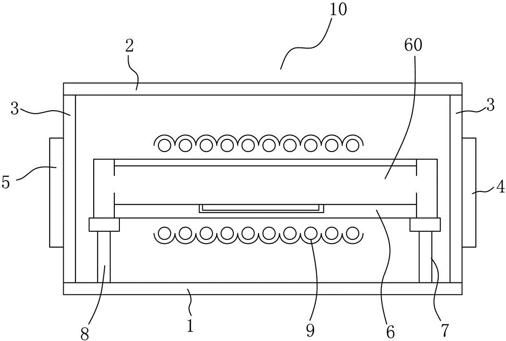
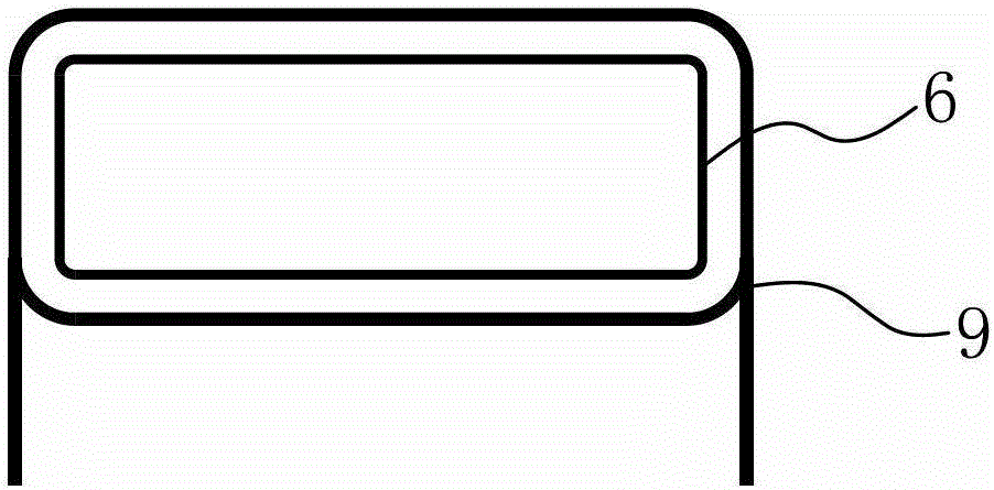
[0040] see Figure 1-2 As shown, this is a specific structure of a preferred example of the present invention, which is a high-temperature large-area silicon carbide epitaxial growth device, including a rectangular parallelepiped (or cube) working chamber 10, the working chamber 10 is composed of: chassis 1, The upper cover 2 and the side wall 3 are surrounded to form a closed space. Wherein, a spare door 4 and a sampling door 5 are respectively arranged on the left and right opposite side walls 3 . Wherein, the sampling door 5 is used to send the sample into the working chamber 10 . The function of the spare door 4 is: when an abnormality occurs in the sampling door 5, related work or maintenance can be continued through the spare door 4 .
[0041] In this embodiment, the chassis 1, the upper cover 2, the side wall 3, the spare door 4 and the s...
PUM
 Abstract
Description
Claims
Application Information
 - R&D
- Intellectual Property
- Life Sciences
- Materials
- Tech Scout
- Unparalleled Data Quality
- Higher Quality Content
- 60% Fewer Hallucinations
Browse by: Latest US Patents, China's latest patents, Technical Efficacy Thesaurus, Application Domain, Technology Topic, Popular Technical Reports.
© 2025 PatSnap. All rights reserved.Legal|Privacy policy|Modern Slavery Act Transparency Statement|Sitemap|About US| Contact US: help@patsnap.com


