
Clock pulse width modulation circuit and clock pulse width modulation method

A technology of width modulation and clock pulse, applied in the field of clock pulse width modulation, which can solve the problems of long clock signal modulation time and large output clock signal jitter, etc.

Active Publication Date: 2012-10-17
成都启臣微电子股份有限公司
View PDF4 Cites 10 Cited by
  • Summary
  • Abstract
  • Description
  • Claims
  • Application Information

AI Technical Summary

Problems solved by technology

[0010] The invention provides a clock pulse width modulation circuit and a clock pulse width modulation method, which solve the technical problems of long modulation time of clock signal and large jitter of output clock signal in the prior art

Method used


Image

  • Clock pulse width modulation circuit and clock pulse width modulation method
  • Clock pulse width modulation circuit and clock pulse width modulation method
  • Clock pulse width modulation circuit and clock pulse width modulation method

Examples


Embodiment Construction

[0096] In the present invention, by tracking a transition edge of the clock signal to be modulated, one transition edge of the output clock signal is obtained, and only the other transition edge within one clock cycle is modulated, effectively reducing the modulation time, and using The charge pump loop and the delay trigger circuit modulate the second jump edge in one clock cycle, so that an output clock signal with higher precision and less jitter can be obtained.

[0097] The specific implementation of the present invention will be described in detail below in conjunction with the accompanying drawings.

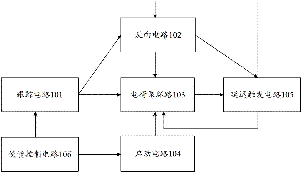
[0098] see figure 1 , figure 1 It is a structural schematic diagram of the clock pulse width modulation circuit of the present invention. figure 1 Among them, the clock pulse width modulation circuit includes: tracking circuit 101, reverse circuit 102, charge pump loop 103, startup circuit 104, delay trigger circuit 105 and enable control circuit 106;

[0099] The tr...


PUM


Abstract

The invention provides a clock pulse width modulation circuit and a clock pulse width modulation method. In the invention, an edge in one clock period of an output clock signal is generated by tracking one edge in one clock period of a to-be-modulated clock period, and another edge in one clock signal of the output clock signal is modulated directly by an initialized modulation circuit so as to obtain the output clock signal. The technical scheme provided by the invention can provide the output clock signal with high accuracy, low jitter and short locking time for a high-speed analog / digital conversion system on the premise of ensuring small chip area occupied by the modulation circuit.

Description

technical field [0001] The present invention relates to the technical field of clock pulse width modulation, in particular to a clock pulse width modulation method and a clock pulse width modulation circuit. Background technique [0002] In the case of the development of very large scale integration (VLSI) towards high speed and low voltage, many high-speed analog-to-digital (A / D) converters use double data rate technology to obtain greater data throughput. Among them, pipeline Analog-to-digital converters are favored by many designers for their high-speed and high-precision features. In the design of pipeline analog-to-digital converters, the accuracy and jitter characteristics of the clock signal duty cycle have an increasing impact on the conversion accuracy of the circuit system with the increase in frequency and conversion bits, and the clock that provides high-precision duty cycle and low jitter Signals are even more important. Clock pulse width modulation technology...

Claims


Application Information

Patent Timeline
Patent Type & Authority Applications(China)
IPC IPC(8): H03K7/08
Inventor 朱樟明王静宇
Owner 成都启臣微电子股份有限公司
Learn More