


Quick Research
Generate reliable direction feasibility study reports for your R&D in just a few steps.

Technical Q&A
Discover and master advanced knowledge NOW. Basics, ideas, possibilities, all at once.

Find Solutions
As an expert in R&D theories, this can generate solutions to your technical problems instantly.

Evaluate Feasibility
Analyze your overall solution with one click, know your potential R&D risks in advance.

Monitor Landscape
Get weekly tech updates, stay abreast of the latest tech innovations and key insights.
Preparation method of ZnTe/GaAs heteroepitaxial layer
A heteroepitaxial, zinc telluride technology, applied in the direction of final product manufacturing, sustainable manufacturing/processing, climate sustainability, etc., can solve the problems that affect the application, the deviation of the zinc telluride epitaxial layer from the ideal stoichiometry, affect the epitaxy Layer crystal quality and other issues, to achieve the effect of wide application prospects
- Summary
- Abstract
- Description
- Claims
- Application Information
AI Technical Summary
Problems solved by technology
Method used
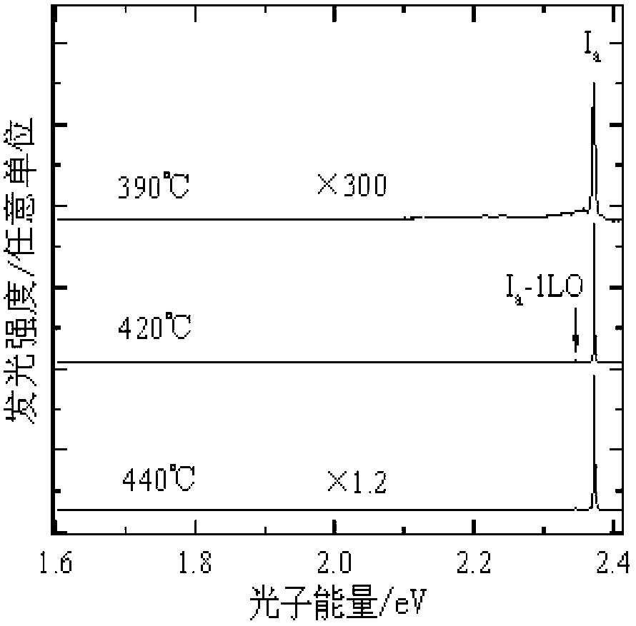
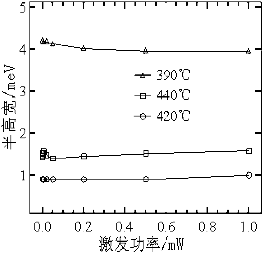
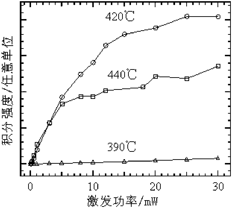
Image

Examples
Embodiment 1
[0043] A method for preparing a zinc telluride / gallium arsenide heteroepitaxial layer, using a metal organic chemical vapor phase epitaxy process, using dimethyl zinc and diethyl tellurium as metal organic sources, using hydrogen as a carrier gas, and using metal organic chemistry Vapor phase epitaxy equipment grows zinc telluride epitaxial layer on gallium arsenide substrate; the process conditions are as follows:
[0044] Reaction chamber background vacuum degree: 1×10 -7 Torr;
[0045] Substrate temperature during growth: 420°C;
[0046] Transport rate of dimethyl zinc: 15μmol / min;
[0047] Transport rate of diethyl tellurium: 15 μmol / min;
[0048] The operation steps of above-mentioned preparation method are as follows:
[0049]1. Cleaning of the GaAs substrate: chemically clean the polished (100) GaAs, ultrasonically clean it in acetone for 5 minutes, and place it in a H 2 SO 4 、H 2 o 2 and H 2 O was etched at 60°C for 20 seconds in a solution composed of a ratio...
Embodiment 2
[0055] The process conditions are as follows:
[0056] Reaction chamber background vacuum degree: 1.2×10 -7 Torr;
[0057] Substrate temperature during growth: 410°C;
[0058] Transport rate of dimethyl zinc: 10 μmol / min;
[0059] Transport rate of diethyl tellurium: 10 μmol / min;
[0060] Growth time: 4 hours;
[0061] ZnTe / GaAs epitaxial layer prepared by MOVPE process, the steps are as follows:
[0062] 1. Cleaning of the GaAs substrate: chemically clean the polished (100) GaAs, ultrasonically clean it in acetone for 5 minutes, and place it in a H 2 SO 4 、H 2 o 2 and H 2 O (according to the ratio of 5:1:1) was etched at 50°C for 20 seconds, and finally rinsed with deionized water;
[0063] 2. Pump the MOVPE equipment reaction chamber into a high vacuum state with a vacuum degree of 1.2×10 -7 Torr, the substrate is heated to 550 ° C for 35 minutes to remove the oxide on the surface of the GaAs substrate;
[0064] 3. Control the substrate temperature at 410°C, adju...
Embodiment 3
[0067] The process conditions are as follows:
[0068] Reaction chamber background vacuum degree: 0.8×10 -7 Torr;
[0069] Substrate temperature during growth: 430°C;
[0070] Transport rate of dimethyl zinc: 30μmol / min;
[0071] Transport rate of diethyl tellurium: 30μmol / min;
[0072] Growth time: 2 hours;
[0073] ZnTe / GaAs epitaxial layer prepared by MOVPE process, the steps are as follows:
[0074] 1. Cleaning of the GaAs substrate: chemically clean the polished (100) GaAs, ultrasonically clean it in acetone for 5 minutes, and place it in a H 2 SO 4 、H 2 o 2 and H 2 O (according to the ratio of 5:1:1) was etched at 70°C for 20 seconds, and finally rinsed with deionized water;
[0075] 2. Pump the MOVPE equipment reaction chamber into a high vacuum state with a vacuum degree of 0.8×10 -7 Torr, the substrate is heated to 600 ° C for 40 minutes to remove the oxide on the surface of the GaAs substrate;
[0076] 3. Control the substrate temperature at 430°C, adjust...
PUM
 Abstract
Description
Claims
Application Information
 - R&D Engineer
- R&D Manager
- IP Professional
- Industry Leading Data Capabilities
- Powerful AI technology
- Patent DNA Extraction
Browse by: Latest US Patents, China's latest patents, Technical Efficacy Thesaurus, Application Domain, Technology Topic, Popular Technical Reports.
© 2024 PatSnap. All rights reserved.Legal|Privacy policy|Modern Slavery Act Transparency Statement|Sitemap|About US| Contact US: help@patsnap.com