Semiconductor module
A technology of semiconductors and casings, which is applied in the fields of semiconductor devices, semiconductor/solid-state device components, and electric solid-state devices, etc., can solve the problems of increased manufacturing costs and high prices
- Summary
- Abstract
- Description
- Claims
- Application Information
AI Technical Summary
Problems solved by technology
Method used
Image

Examples
Embodiment approach 1
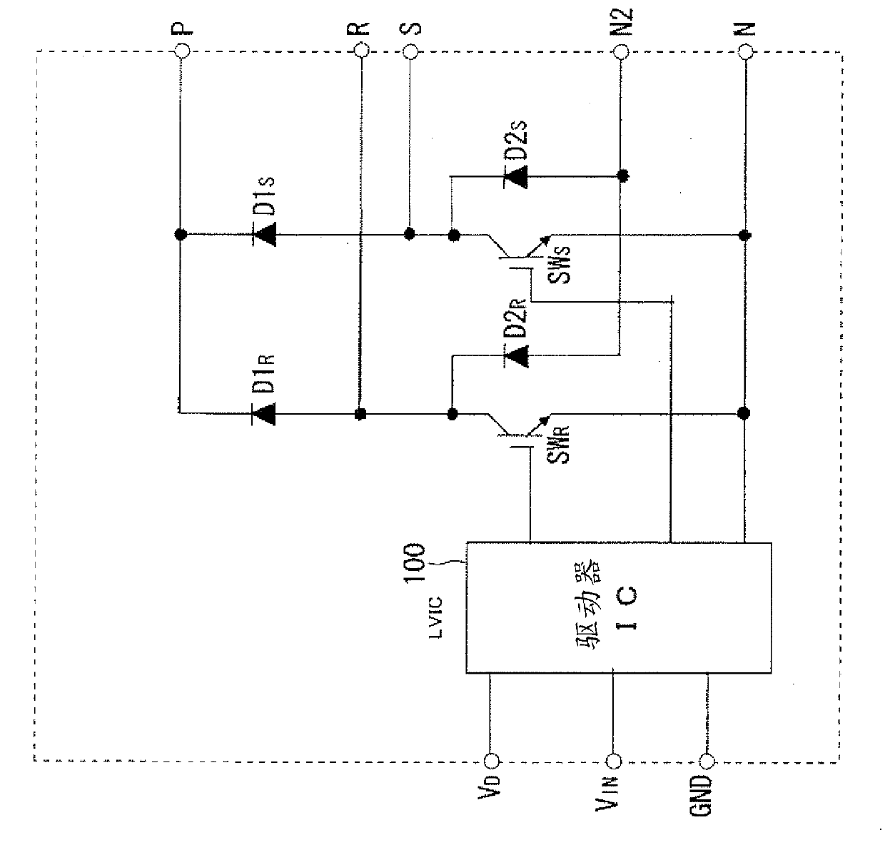
[0022] figure 1 It is a circuit diagram of a PFC module which is a semiconductor module of the present invention. As shown in the figure, the PFC module has: first to fourth diodes D1 R , D1 S 、D2 R 、D2 S Diode bridge constituted; first and second switching elements SW for power factor improvement R 、SW S ; Control the first and second switching elements SW R 、SW S driver IC100.
[0023] The diode bridge is constructed as follows: a first and a second diode D1 with upper arms whose cathodes are connected to each other R , D1 S And the third and fourth diodes D2 of the lower arm whose anodes are connected to each other R 、D2 S , the first diode D1 R and the third diode D2 R connected in series and the second diode D1 S and the fourth diode D2 S connected in series. first diode D1 R anode of the third diode D2 and R The cathode of the R terminal is connected, and the second diode D1 S anode of the fourth diode D2 and S The S terminal to which the cathode is c...
Embodiment approach 2
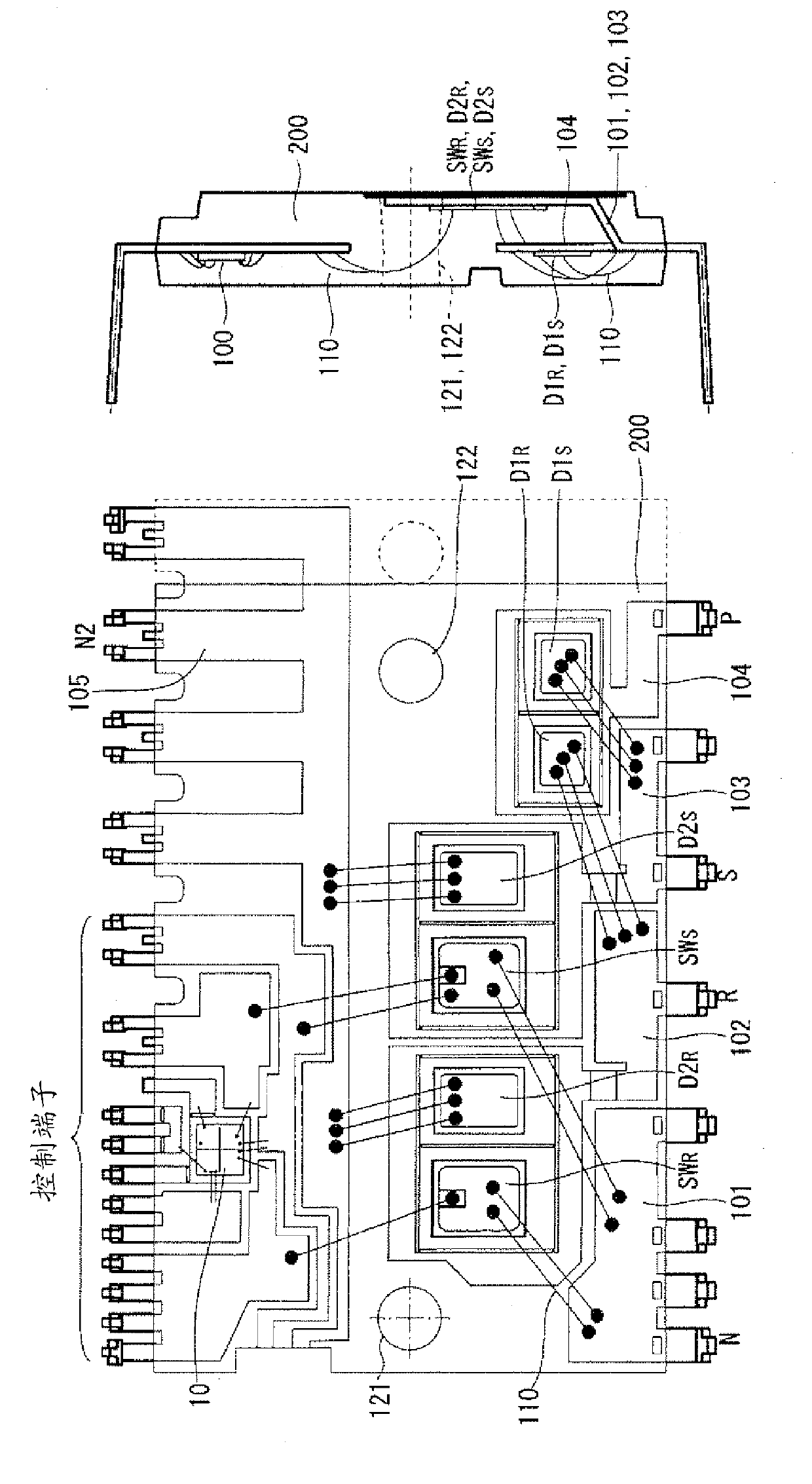
[0036] Figure 4 It is a block diagram of the PFC module of Embodiment 2. In this embodiment, inside the housing 200, the first and second diodes D1 as SiC devices R , D1 S Distributed in the third and fourth diodes D2 R 、D2 S and the first and second switching elements SW R 、SW S outside. That is, the first and second diodes D1 R , D1 S It is arranged near one side surface of the case 200 where the lead frames 101 to 104 protrude. In addition, as in Embodiment 1, the first and second diodes D1 are mounted R , D1 S The first lead frame 104 is not downward inside the housing 200 (the first and second diodes D1 R , D1 S perpendicular to the mounting surface) is bent.
[0037] According to this configuration, the first and second diodes D1 can be connected R , D1 S The lead wire wiring 110 of the lead frames 102 and 103 is shortened. The length of the wire wiring 110 affects the surge current tolerance of the PFC module, and shortening it can improve the surge cur...
Embodiment approach 3
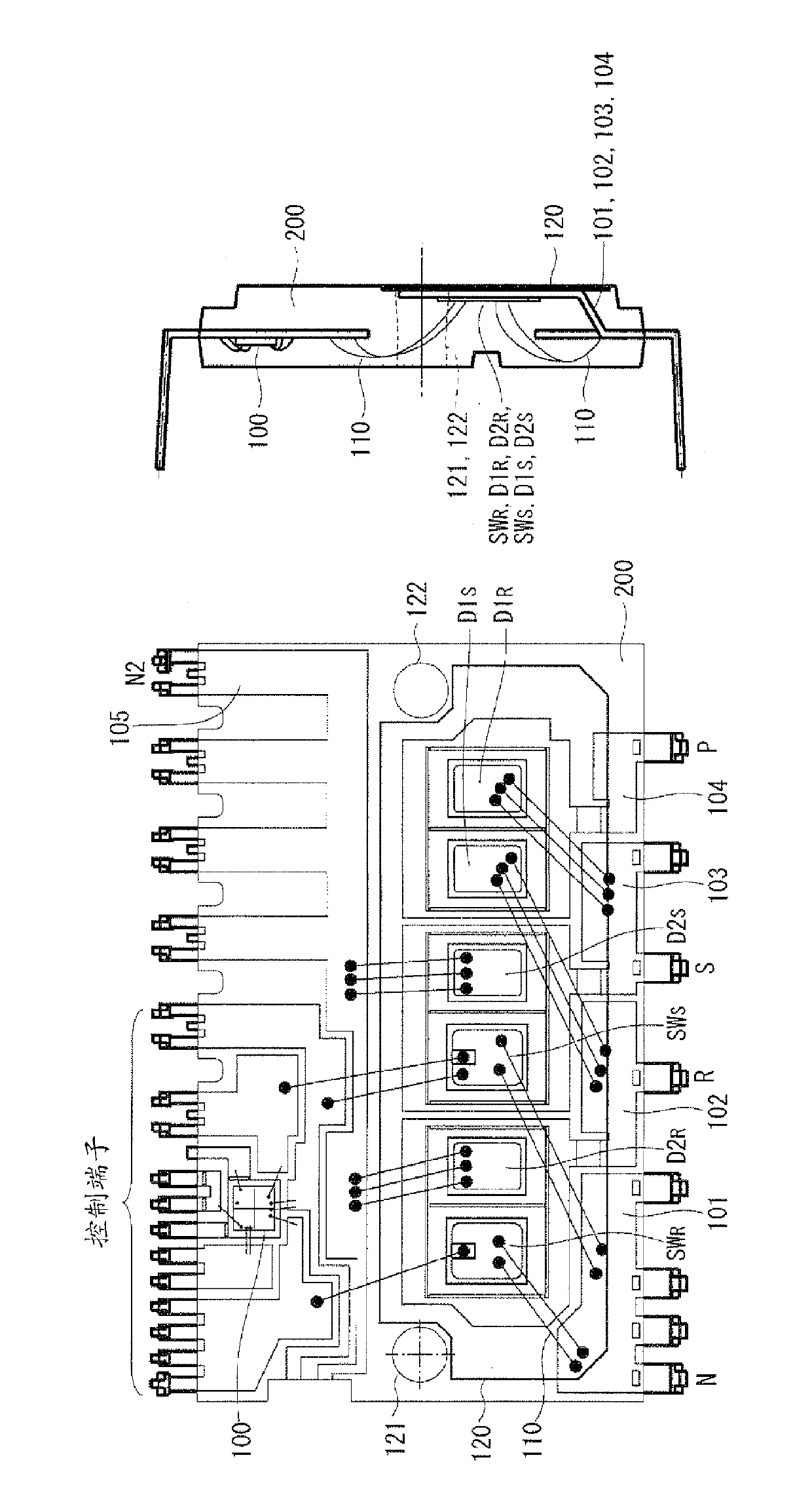
[0039] Figure 5 It is a block diagram of the PFC module of Embodiment 3. In this embodiment, as in Embodiment 2, inside the housing 200, the first and second diodes D1 as SiC devices are R , D1 S Distributed in the third and fourth diodes D2 R 、D2 S and the first and second switching elements SW R 、SW S outside (the vicinity of one side surface of the housing 200 where the lead frames 101 to 104 protrude).
[0040] In addition, the SiC device has low resistance, so it is possible to reduce the size of the chip. For example, in a module with a rated value of 600V·20A (rms), the first and second diodes D1 can be R , D1 S The chip size becomes about half. Therefore, if the first and second diode D1 R , D1 S Closer to the outer side, a space is formed in the central portion of the housing 200 . In this embodiment, the through-hole 122 is arranged in this space. That is, in a plan view, the first and second diodes D1 R , D1 S At least one of them is disposed between...
PUM
 Abstract
Description
Claims
Application Information
 - R&D
- Intellectual Property
- Life Sciences
- Materials
- Tech Scout
- Unparalleled Data Quality
- Higher Quality Content
- 60% Fewer Hallucinations
Browse by: Latest US Patents, China's latest patents, Technical Efficacy Thesaurus, Application Domain, Technology Topic, Popular Technical Reports.
© 2025 PatSnap. All rights reserved.Legal|Privacy policy|Modern Slavery Act Transparency Statement|Sitemap|About US| Contact US: help@patsnap.com