Side wall and method for forming side wall and semiconductor

A sidewall and process technology, applied in semiconductor/solid-state device manufacturing, electrical components, circuits, etc., can solve problems such as field effect transistor failure, and achieve the effect of avoiding failure

Active Publication Date: 2012-08-15
SHANGHAI HUAHONG GRACE SEMICON MFG CORP
View PDF6 Cites 0 Cited by
  • Summary
  • Abstract
  • Description
  • Claims
  • Application Information

AI Technical Summary

Problems solved by technology

[0011] However, in the prior art, when the performance of the field effect transistor whose sidewall material is all silicon oxide is tested, it is found that the field effect transistor fails
[0012] In the prior art, there are many methods for forming sidewalls, such as the method for forming sidewalls disclosed in the patent document with publication number CN101599429A, but none of them solves the above technical problems

Method used


Image

  • Side wall and method for forming side wall and semiconductor
  • Side wall and method for forming side wall and semiconductor
  • Side wall and method for forming side wall and semiconductor

Examples


Embodiment Construction

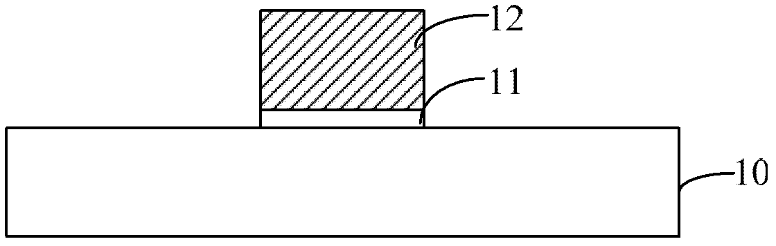
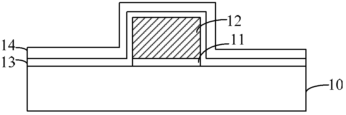
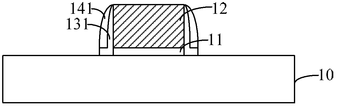
[0059] In the prior art, in the process of forming a field effect crystal, the specific process of forming a metal silicide is: provide a silicon substrate, and form a layer of silicon oxide on the silicon substrate; then, form a photolithographic process on the silicon oxide. After that, the photoresist layer is exposed and developed to form a pattern in the photoresist layer, which defines the pattern of the oxide of silicon to be etched; after that, the patterned photoresist layer For mask wet etching of silicon oxide, the pattern of the photoresist layer is transferred to the silicon oxide layer to form a self-aligned metal silicide block; then, the patterned photoresist layer is removed, and self-aligned The metalloid silicide block is used as a mask to react metals such as cobalt, nickel, titanium and silicon with silicon on the gate, source and drain to form metal silicide. In the process of wet etching silicon oxide to form SAB, due to the corrosiveness of the etching ...


PUM


Abstract

The invention relates to a side wall and a method for forming the side wall and a semiconductor. The method for forming the side wall comprises the following steps of: providing a substrate with a grid electrode structure, wherein the grid electrode structure comprises a grid electrode and a gate dielectric layer which is located between the grid electrode and the substrate; forming a first dielectric layer which covers the substrate and the gate dielectric layer and is a single-layer or laminated structure; forming a second dielectric layer on the first dielectric layer, wherein the corrosion resistance of the second dielectric layer on an etching liquid used in the process of forming a self-alignment metal silicide block is more than that of the outermost layer material of the first dielectric layer on the etching liquid; and sequentially etching the second dielectric layer and the first dielectric layer to form the side wall at the periphery of the grid electrode. The side wall formed in the invention has large corrosion resistance on a solution utilized in the washing process of the formed side wall, thus the loss of the side wall in the process of forming the self-alignment metal silicide block can be reduced, the corresponding side wall width is increased, and the field effect transistor failure problem caused by too small side wall can be avoided.

Description

technical field [0001] The invention relates to the field of semiconductor technology, in particular to a method for forming a side wall and a semiconductor device. Background technique [0002] In the semiconductor devices of the prior art, the sidewall structure usually formed around the gate is an ONO (oxide-nitride-oxide) structure. However, due to the relatively large dielectric constant k of silicon nitride in the ONO structure, in some devices such as When a small capacitance is required between the gate, the source, and the drain of a radio frequency device, the sidewalls around the gate cannot use ONO structure sidewalls, and need to use sidewalls made of silicon oxide. [0003] In the semiconductor process of the prior art, the process steps of the method for forming a semiconductor device whose material is silicon oxide are: [0004] refer to figure 1 , provide substrate 10; form gate dielectric layer 11 on this substrate 10; form gate 12 on gate dielectric laye...

Claims


Application Information

Patent Timeline
IPC IPC(8): H01L21/336H01L21/02H01L21/316
Inventor 李乐
Owner SHANGHAI HUAHONG GRACE SEMICON MFG CORP
Why Eureka
Try Eureka