Detecting structure and detecting method for temperature coefficient of resistance (TCR)
A technology of resistance temperature coefficient and detection structure, which is applied in the direction of single semiconductor device testing, etc., can solve the problems of complex process, long time and time-consuming heating of the device under test, etc., achieve rapid heating, not easy to electromigration failure, and improve the detection resistance temperature The effect of the coefficient
- Summary
- Abstract
- Description
- Claims
- Application Information
AI Technical Summary
Problems solved by technology
Method used
Image

Examples
no. 1 example
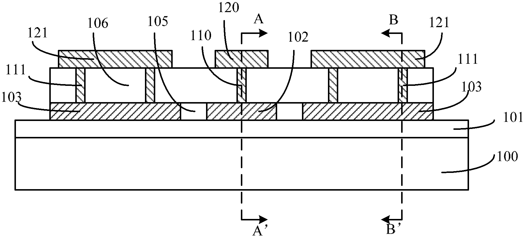
[0074] Please refer to figure 1 , which is a schematic cross-sectional view of the temperature coefficient of resistance detection structure described in this embodiment, including:
[0075] A semiconductor substrate 100 ; a device under test 102 located on the surface of the semiconductor substrate 100 , the material of the device under test 102 is polysilicon.
[0076] The role of the semiconductor substrate 100 is to provide a working platform for the subsequent formation of semiconductor devices, and the materials of the semiconductor substrate 100 are n-type silicon, p-type silicon, silicon on insulating layer (SOI), silicon nitride and gallium arsenide and other III-V compounds, etc.
[0077] The device under test 102 can be a device such as a micro-actuator or a microsensor in a MEMS semiconductor device; between the semiconductor substrate 100 and the device under test 102, according to the process requirements of a specific semiconductor device, there can also be Se...
no. 2 example
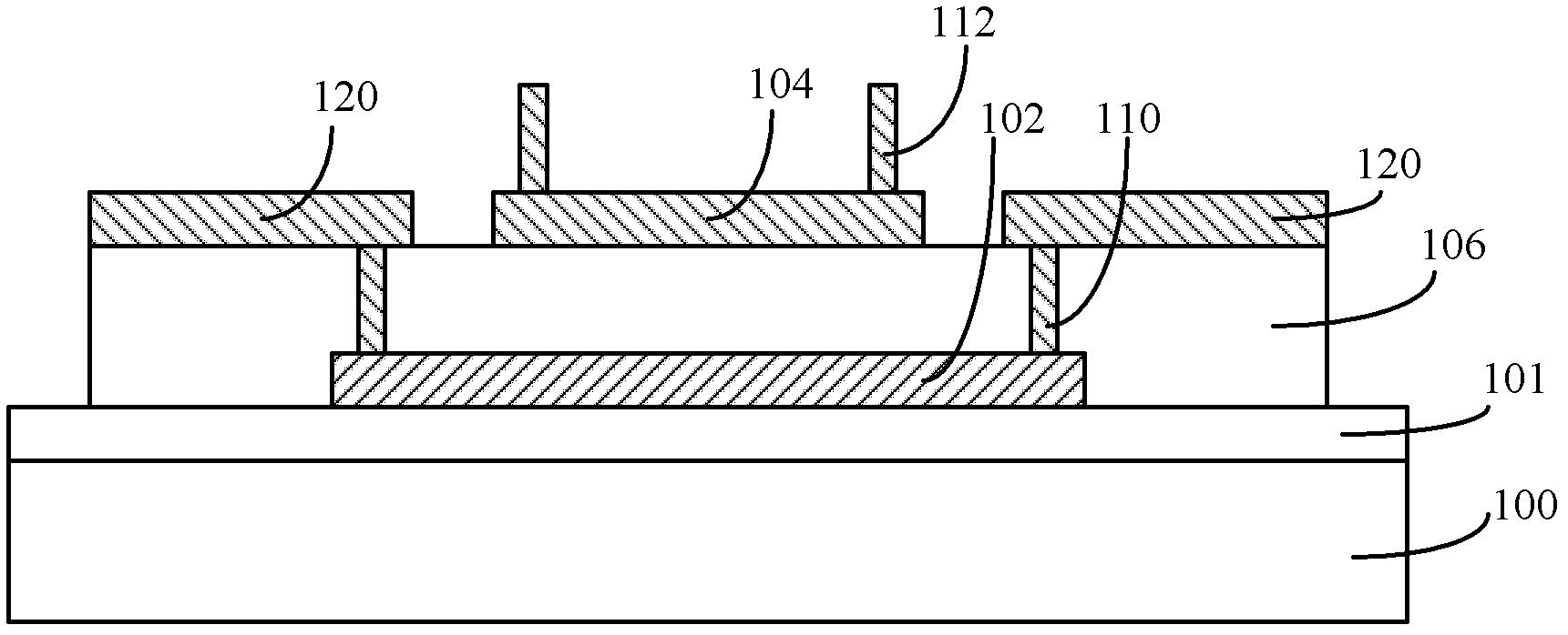
[0115] Please refer to Figure 4 , which is a schematic cross-sectional view of the temperature coefficient of resistance detection structure described in this embodiment, including:
[0116] A semiconductor substrate 200 ; a device under test 202 located on the surface of the semiconductor substrate 200 , and the material of the device under test 202 is polysilicon.
[0117] The functions and materials of the semiconductor substrate 200 are the same as those described in the first embodiment, and will not be repeated here.
[0118] The device under test 202 may be a micro-actuator, a micro-sensor and other devices in a MEMS semiconductor device;
[0119] Between the semiconductor substrate 200 and the device under test 202, according to the process requirements of specific semiconductor devices, there may also be several polysilicon device layers electrically isolated by isolation layers.
[0120] In this embodiment, there is a dielectric layer 201 between the semiconductor...
no. 3 example
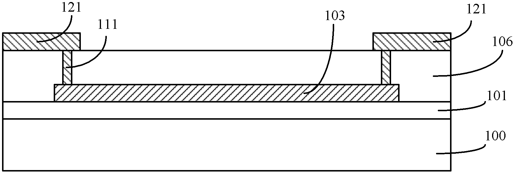
[0153] Please refer to Figure 5 , which is a schematic cross-sectional view of the temperature coefficient of resistance detection structure described in this embodiment, including:
[0154] A semiconductor substrate 300 ; a device under test 302 located on the surface of the semiconductor substrate 300 , and a material of the device under test 302 is polysilicon.
[0155] The functions and materials of the semiconductor substrate 300 are the same as those described in the first embodiment, and will not be repeated here.
[0156] The device under test 302 may be a micro-actuator, a micro-sensor and other devices in a MEMS semiconductor device;
[0157] Between the semiconductor substrate 300 and the device under test 302, according to the process requirements of specific semiconductor devices, there may also be several polysilicon device layers electrically isolated by insulating layers.
[0158] In this embodiment, there is a dielectric layer 301 between the semiconductor ...
PUM
 Abstract
Description
Claims
Application Information
 - R&D
- Intellectual Property
- Life Sciences
- Materials
- Tech Scout
- Unparalleled Data Quality
- Higher Quality Content
- 60% Fewer Hallucinations
Browse by: Latest US Patents, China's latest patents, Technical Efficacy Thesaurus, Application Domain, Technology Topic, Popular Technical Reports.
© 2025 PatSnap. All rights reserved.Legal|Privacy policy|Modern Slavery Act Transparency Statement|Sitemap|About US| Contact US: help@patsnap.com