Method for introducing strain to channel and device manufactured by the same

A channel and compressive strain technology, applied in semiconductor devices, semiconductor/solid-state device manufacturing, electrical components, etc., can solve problems such as channel introduction defects, complex processes, and weakening of induced strain effects, and achieve simple process complexity and strong The effect of process flexibility

Active Publication Date: 2012-07-18
INST OF MICROELECTRONICS CHINESE ACAD OF SCI
View PDF5 Cites 2 Cited by
  • Summary
  • Abstract
  • Description
  • Claims
  • Application Information

AI Technical Summary

Problems solved by technology

However, some of the above-mentioned methods of generating channel local strain and changing the type of channel stress require complex processes, and some are easy to introduce defects into the channel. On the other hand, with the continuous shrinking of device feature size, The induced strain effect is also weakening

Method used


Image

  • Method for introducing strain to channel and device manufactured by the same
  • Method for introducing strain to channel and device manufactured by the same
  • Method for introducing strain to channel and device manufactured by the same

Examples


no. 1 example

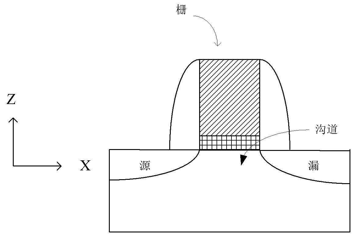
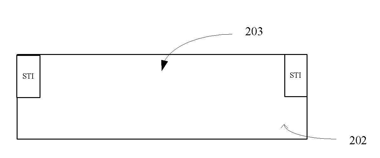
[0014] This embodiment gives the steps of making an NMOS device by using this method. A semiconductor substrate 202 is provided, which may be of any type known in the electronics field, such as bulk semiconductor, semiconductor-on-insulator (SOI). And the semiconductor substrate may be strained, unstrained, or contain strained or unstrained regions therein. After the semiconductor substrate is provided, an isolation region is formed in the semiconductor substrate 202 by using conventional techniques well known in the art. The isolation region is, for example, a trench isolation region (STI) or a field isolation region. In addition, the isolation region material Can be stressed material or unstressed material.

[0015] A channel 203 is formed on the semiconductor substrate in the active region between the isolation regions, such as Figure 2a shown.

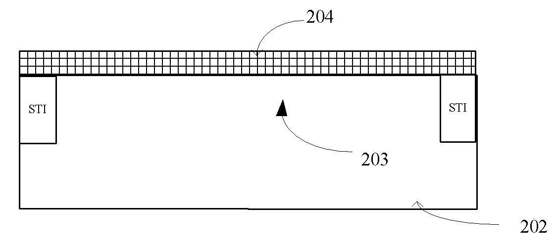
[0016] A gate dielectric layer 204 is formed on the channel, such as Figure 2b As shown, the material of the gate dielectri...

no. 2 example

[0030] This embodiment gives the steps of making a PMOS device by using this method. A semiconductor substrate 302 is provided, and the semiconductor substrate may be of any type known in the field of electronics, such as bulk semiconductor, semiconductor-on-insulator (SOI). And the semiconductor substrate may be strained, unstrained, or contain strained or unstrained regions therein. After the semiconductor substrate is provided, an isolation region is formed in the semiconductor substrate 302 by using conventional techniques well known in the art. The isolation region is, for example, a trench isolation region (STI) or a field isolation region. In addition, the isolation region material Can be stressed material or unstressed material.

[0031] A channel 303 is formed on the semiconductor substrate in the active region between the isolation regions, such as Figure 3a shown.

[0032] A gate dielectric layer 304 is formed on the channel, such as Figure 3b As shown, the ma...


PUM


Abstract

The invention relates to a method for introducing strain to a channel of a MOS (Metal Oxide Semiconductor) device and a device manufactured by the method. The method comprises the following steps of: providing a semiconductor substrate; forming a channel on the semiconductor substrate; forming a first grid dielectric layer on the channel; forming a polycrystalline silicon grid electrode layer on the first grid dielectric layer; doping or injecting a first element in the polycrystalline silicon grid electrode layer; removing parts of the first grid dielectric layer and the polycrystalline silicon grid electrode layer so as to form a first grid electrode structure; forming a source drain extending zone in the channel; forming side walls on both sides of the first grid electrode structure; forming a source drain electrode in the channel; and annealing so that polycrystalline silicon doped or injected with the first element generates crystal lattice variation in a high-temperature crystallization process, thus generating first strain in the polycrystalline silicon grid electrode layer, and introducing the first stress to the channel through a grid medium layer. The method has stronger process flexibility, simpler process complication and no additional process cost.

Description

technical field [0001] The invention relates to a method for introducing strain into a channel and a device made by the method. Background technique [0002] Theoretical and empirical studies have confirmed that when stress is applied to the channel of a transistor, the semiconductor lattice in the channel region is strained, and the carrier mobility of the transistor can be increased or decreased; however, it is also known that the electron and space Caves respond differently to the same type of strain. For example, compressive stress is applied in the longitudinal direction of current flow to cause compressive strain in the channel region, which is beneficial to improve hole mobility, but correspondingly reduces electron mobility. Applying tensile stress in the longitudinal direction leads to tensile strain in the channel region, which is beneficial to improve electron mobility, but correspondingly reduces hole mobility. With the continuous reduction of device feature si...

Claims


Application Information

Patent Timeline
IPC IPC(8): H01L21/336H01L21/283H01L29/78H01L29/51
CPCH01L29/66545H01L29/7847H01L29/7845
Inventor 殷华湘徐秋霞陈大鹏
Owner INST OF MICROELECTRONICS CHINESE ACAD OF SCI
Why Eureka
Try Eureka