Ceramic capacitor structure

A ceramic capacitor and capacitor technology, applied in multiple fixed capacitors, fixed capacitor terminals, fixed capacitor components and other directions, can solve the problems of reduced automation, time-consuming and cost-consuming, and inaccurate positioning effects. The effect of pulling force, improving bonding force, and reducing height

Inactive Publication Date: 2012-07-18
HOLY STONE ENTERPRISE
View PDF5 Cites 8 Cited by
  • Summary
  • Abstract
  • Description
  • Claims
  • Application Information

AI Technical Summary

Problems solved by technology

[0005] However, with the development trend of high-density integrated circuits and stronger functions, the size of ceramic capacitors must also be made smaller and smaller. The standard operating procedure for existing ceramic capacitors is to use two metal wires C to use artificial plug-ins or Manual post-soldering is used for the production of downstream products. This kind of production method using metal wire C will reduce the degree of automation. In addition to requiring a lot of manual plug-in to the circuit board and welding procedures, it will consume more man-hours and In addition to greatly increasing the cost, the manual insertion must also be quite accurate, otherwise the metal wire C will be easily squeezed, deformed or broken due to the difficulty in assembly, not only the overall production efficiency is poor, and the positioning effect is not accurate, And because the existing ceramic capacitor is a vertical plug-in circuit board, its height will be limited by the diameter of the internal ceramic capacitor A, so that the height cannot be effectively reduced, so under the consideration of the actual use of downstream products, if it can Developed a ceramic capacitor structure redesign to improve the original use of such ceramic capacitors requires a lot of man-hours and costs, so that ceramic capacitors can be automated production towards chip and surface mount technology (SMT) welding, In addition to accelerating the production speed of downstream products, it can also save a lot of labor costs, which needs to be redesigned and effectively solved by those engaged in this industry

Method used


Image

  • Ceramic capacitor structure
  • Ceramic capacitor structure
  • Ceramic capacitor structure

Examples


Embodiment Construction

[0034] In order to achieve the above-mentioned purpose and effect, the technical means and the structure thereof adopted in the present invention are hereby illustrated in detail with respect to the preferred embodiments of the present invention. Its features and functions are as follows, so as to fully understand.

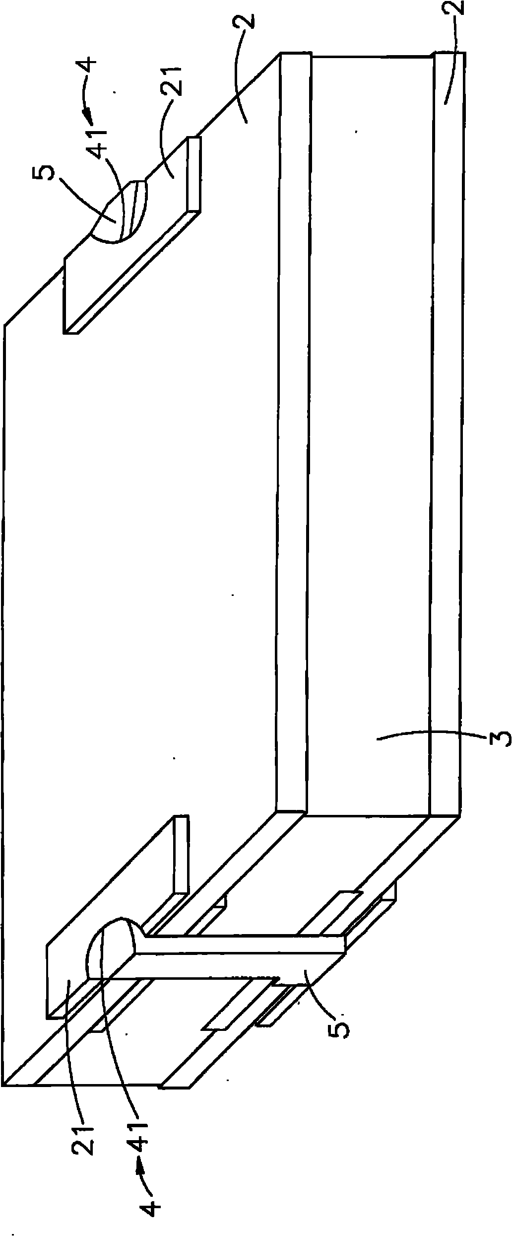
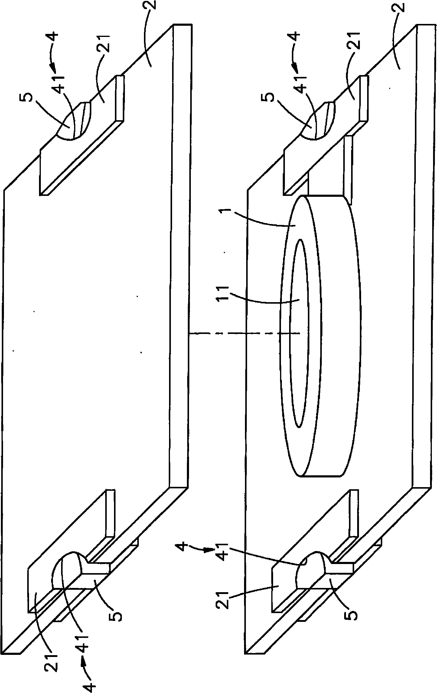
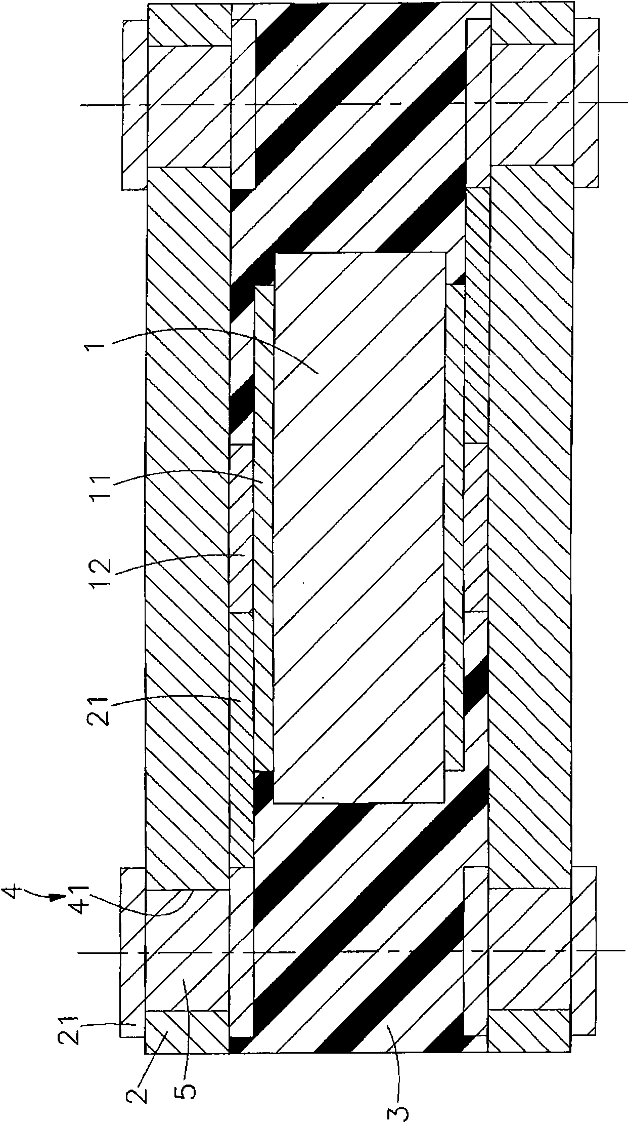
[0035] see Figure 1 to Figure 5As shown, they are the three-dimensional appearance diagram, the three-dimensional exploded view, the side sectional view, the manufacturing flow chart and the three-dimensional exploded view of the preferred embodiment of the present invention. It can be clearly seen from the figure that the present invention includes one or one The above capacitor base material 1 and a plurality of carrier plates 2, wherein the capacitor base material 1 is positioned at the opposite inner side of the two carrier plates 2, and has metal on the two side surfaces of the capacitor base material 1 that can be opposite to the inner surface of the second ...


PUM


Abstract

The invention discloses a ceramic capacitor structure, which comprises one or more capacitor substrates and a plurality of support plates, wherein the capacitor substrates are positioned on opposite inner sides of every two support plates respectively; electrode conductors on two side surfaces of the capacitor substrates are electrically connected with metal circuit layers on opposite inner side surfaces of the two support plates respectively, and are in staggered and overlapped states; an insulating layer is molded integrally between each capacitor substrate and the inside of each support plate; slots for exposing the metal circuit layers are longitudinally formed on two vertical side planes of each insulating layer respectively; and the surfaces of the slots and the support plates are provided with outer end part electrodes which are covered on the metal circuit layers and are connected electrically. By means of a large-area circuit layout design with a plurality of support plates, a plurality of capacitor substrates can be connected in parallel on a single main body according to the requirements of a manufacturer, and the effects of reducing area and increasing capacitance value are achieved in a modular laminating way in accordance with the manufacturing specification of a ceramic capacitor simultaneously, so that quick volume production can be more simply and easily performed, and the cost can be saved effectively.

Description

technical field [0001] The present invention provides a ceramic capacitor structure, in particular, multiple capacitor base materials can be arranged in parallel on a single body by utilizing the circuit layout design of multiple substrates, and present a stacked state of interlaced stacking, so as to achieve reduced area, The effect of increasing the capacitance value can also speed up production and save labor costs. Background technique [0002] Today's electronic products and their peripheral related electronic equipment all use active components and passive components. Active components (such as microprocessors or chips, etc.) are functions that can perform calculations and processing independently, while passive components are When the current or voltage is changed, the resistance or impedance of the component will not change accordingly, and the resistance, capacitance and inductance are collectively called the three passive components, and the three can be used in in...

Claims


Application Information

Patent Timeline
IPC IPC(8): H01G4/38H01G4/228
Inventor 方又正
Owner HOLY STONE ENTERPRISE
Why Eureka
Try Eureka