Silicon nano-wire array or silicon nano-pore array Schottky junction type solar battery and preparation method thereof
A technology of silicon nanowire arrays and solar cells, which is applied in circuits, photovoltaic power generation, electrical components, etc., can solve the problems that limit the wide application of solar cells, the effect of anti-reflection layer is not very obvious, and restrict the efficiency of solar cells. Effects of weak absorption capacity, efficiency improvement, and low cost
- Summary
- Abstract
- Description
- Claims
- Application Information
AI Technical Summary
Problems solved by technology
Method used
Image
Examples
Embodiment 1
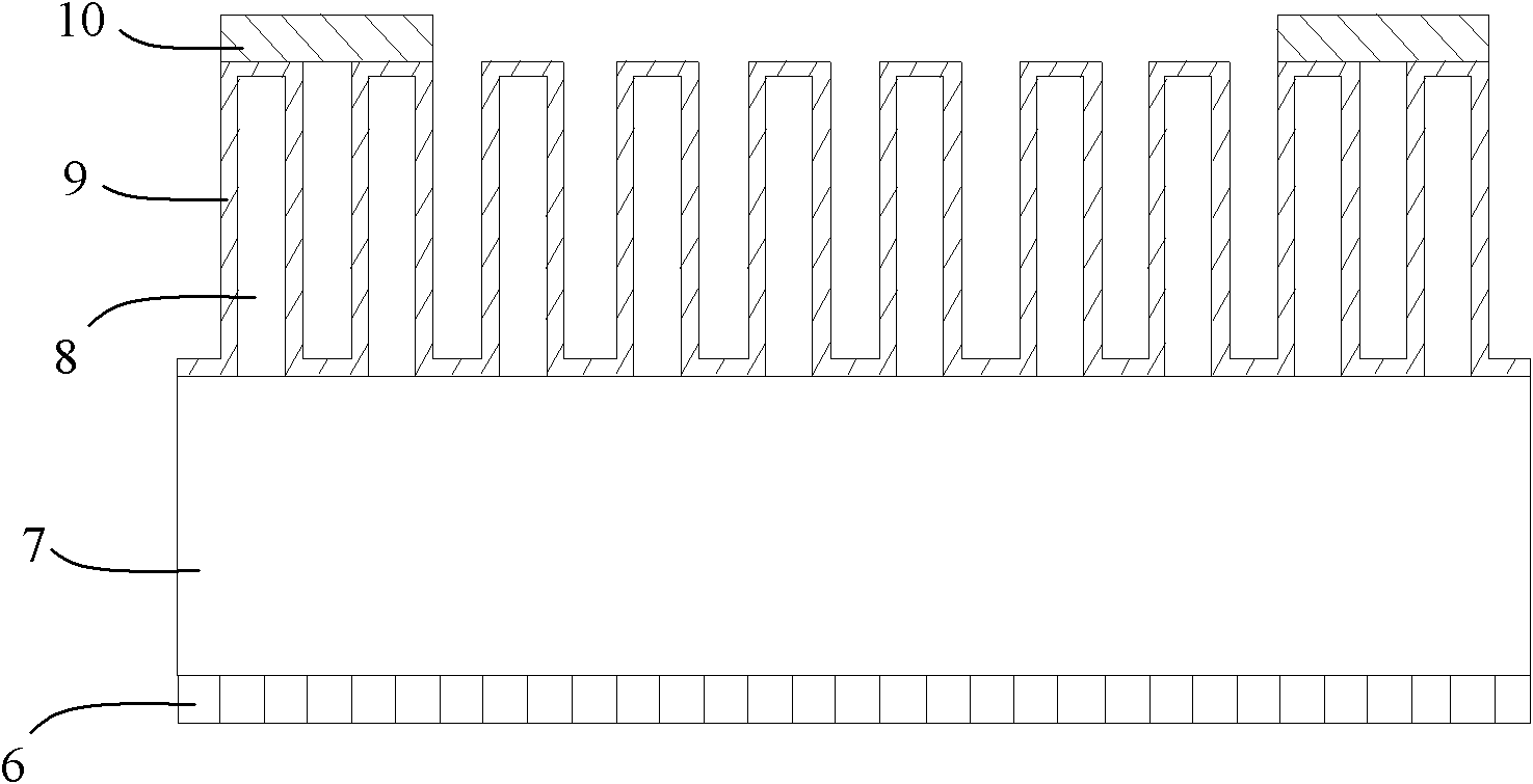
[0021] see figure 1 In this embodiment, the silicon nanowire array or the silicon nanohole array Schottky junction solar cell has the following structure:
[0022] Al metal film back electrode layer 6 is set on the bottom surface of P-type silicon base layer 7, as the back side lead-out electrode; P-type silicon base layer 7 is positioned on Al metal film back electrode layer 6, as the base area of solar cell; P-type silicon The nanowire array layer 8 is located on the upper surface of the P-type silicon base layer 7, the surface of the P-type silicon nanowire array layer 8 is wrapped with a Ti metal layer 9, and the Ti metal layer 9 and the P-type silicon nanowire array layer 8 form a small Tertiary junction; a Ti grid electrode 10 is arranged on the Ti metal layer 9 as a front-side lead-out electrode; a silicon nanowire array or a silicon nanohole array.
[0023] In this embodiment, the preparation method of silicon nanowire array or silicon nanohole array Schottky juncti...
Embodiment 2
[0026] Another example figure 1 As shown, the silicon nanowire array or silicon nanohole array Schottky junction solar cell in this embodiment has the following structure:
[0027] The Ti metal film back electrode layer 6 is set on the bottom surface of the N-type silicon base layer 7, as the back lead-out electrode; the N-type silicon base layer 7 is located on the Ti metal film back electrode layer 6, as the base area of the solar cell; the N-type silicon nanometer The line array layer 8 is located on the upper surface of the N-type silicon base layer 7; the surface of the N-type silicon nanowire array layer 8 is wrapped with an Au metal layer or a Pt metal layer 9, and the Au metal layer or the Pt metal layer 9 and the N-type silicon The nanowire array layer 8 forms a Schottky junction; an Ag grid electrode 10 is set on the Au metal layer or Pt metal layer 9 as a front-side lead-out electrode; the silicon nanowire array or silicon nanohole array.
[0028] In this embodim...
PUM
 Abstract
Description
Claims
Application Information
 - R&D
- Intellectual Property
- Life Sciences
- Materials
- Tech Scout
- Unparalleled Data Quality
- Higher Quality Content
- 60% Fewer Hallucinations
Browse by: Latest US Patents, China's latest patents, Technical Efficacy Thesaurus, Application Domain, Technology Topic, Popular Technical Reports.
© 2025 PatSnap. All rights reserved.Legal|Privacy policy|Modern Slavery Act Transparency Statement|Sitemap|About US| Contact US: help@patsnap.com


