Deep-ultraviolet light emitting diode capable of effectively improving external quantum efficiency and method for preparing deep-ultraviolet light emitting diode
A technology of external quantum efficiency and light-emitting diodes, applied in electrical components, circuits, semiconductor devices, etc., can solve the problem of low external quantum efficiency, achieve high frontal light extraction efficiency, and enhance the effect of radiation recombination probability
- Summary
- Abstract
- Description
- Claims
- Application Information
AI Technical Summary
Problems solved by technology
Method used
Image
Examples
preparation example Construction
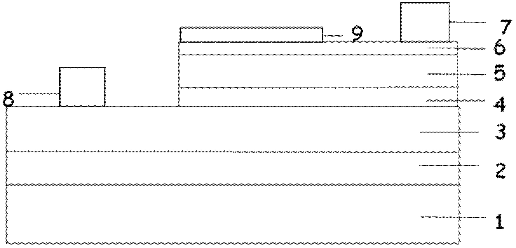
[0023] The preparation method of the deep ultraviolet light-emitting diode that effectively improves the external quantum efficiency comprises the following steps:
[0024] 1) growing an AlN buffer layer 2, an n-AlGaN layer 3, an active layer 4, a p-AlGaN layer 5 and a p-GaN capping layer 6 on a substrate 1;
[0025] 2) Use ICP technology to etch the n-type mesa, and form p-type and n-type ohmic contacts through photolithography, vacuum electron beam evaporation deposition and rapid thermal annealing treatment technology;
[0026] 3) Depositing an aluminum film layer 9 on the p-GaN capping layer 6;
[0027] 4) An n-type electrode 8 is provided on the n-AlGaN layer 3 , and a p-type electrode 7 is provided on the p-GaN capping layer 6 .
[0028] The thickness of the p-GaN cap layer 6 is controlled within 20nm, on the one hand, in order to effectively couple the surface plasmons at the interface with the dipoles in the quantum well, and on the other hand, to weaken the effect of...
Embodiment 1
[0045] Utilize photolithography technology, and then deposit ultra-thin aluminum film structure on the p-GaN cover layer by vacuum electron beam evaporation deposition technology. In the process of preparing the metal thin film, first, pre-program the thickness of the aluminum thin film to be deposited within 10nm, bombard the corresponding aluminum target with an electron gun, heat the material to evaporate and adsorb on the p-GaN capping layer, forming a continuous flat Metallic aluminum film.
Embodiment 2
[0047] Using photolithography technology, aluminum source is used as the target, and then a large number of target atoms are bombarded by magnetron sputtering to deposit a film on the p-GaN cap layer to form an ultra-thin aluminum film structure. The thickness of the aluminum film is Control within 10nm, and use highly integrated automation software for real-time monitoring.
PUM
 Abstract
Description
Claims
Application Information
 - R&D Engineer
- R&D Manager
- IP Professional
- Industry Leading Data Capabilities
- Powerful AI technology
- Patent DNA Extraction
Browse by: Latest US Patents, China's latest patents, Technical Efficacy Thesaurus, Application Domain, Technology Topic, Popular Technical Reports.
© 2024 PatSnap. All rights reserved.Legal|Privacy policy|Modern Slavery Act Transparency Statement|Sitemap|About US| Contact US: help@patsnap.com


