


Quick Research
Generate reliable direction feasibility study reports for your R&D in just a few steps.

Technical Q&A
Discover and master advanced knowledge NOW. Basics, ideas, possibilities, all at once.

Find Solutions
As an expert in R&D theories, this can generate solutions to your technical problems instantly.

Evaluate Feasibility
Analyze your overall solution with one click, know your potential R&D risks in advance.

Monitor Landscape
Get weekly tech updates, stay abreast of the latest tech innovations and key insights.
Maintaining voltage raising method
A technology for maintaining voltage and silicon devices, which is applied to circuits, electrical components, electric solid-state devices, etc., and can solve the problem that the maintenance voltage of devices is difficult to increase
- Summary
- Abstract
- Description
- Claims
- Application Information
AI Technical Summary
Problems solved by technology
Method used
Image

Examples
preparation example Construction
[0020] The SOI high sustaining voltage thyristor device prepared by the preparation process provided by the invention is used as an electrostatic protection device in the field of electrostatic protection, and has excellent electrostatic protection performance. When SOI thyristor with parasitic PNPN, PNPNP or NPNPN structure is applied in the field of electrostatic protection, the minimum voltage required to maintain the device working in the hysteresis region is improved through this process, reducing the risk of device latch-up and improving device reliability.
[0021] A method for increasing the sustain voltage provided by the present invention uses SOI technology to manufacture SOI thyristor devices with parasitic PNPN, PNPNP or NPNPN structures, and embeds such as diodes and diode strings in the parasitic transistor feedback paths of SOI thyristor devices. Semiconductor components such as transistors or MOS tubes that can suppress the positive feedback of the thyristor, ...
Embodiment 1
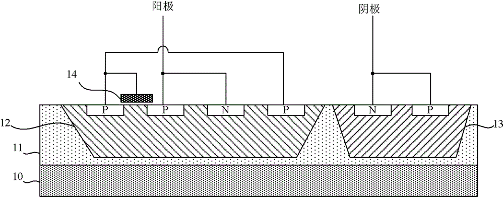
[0025] Such as figure 1 As shown, a kind of SOI high sustain voltage thyristor device made by using the method for increasing the sustain voltage provided by the present invention includes: 10 is a buried oxide layer, and the material is silicon dioxide; 11 is a top oxide layer, which is used to make an SOI device main area of . In this example, an N well 12 and a P well 13 are formed in the P-type doped top oxide layer 11 with appropriate concentrations. As shown in the figure, P-type or N-type impurities are injected to form a high-concentration P+ region or a high-concentration N+ region, and an SOI thyristor device with a PNPN parasitic structure is formed between the anode and the cathode. An embedded PMOS transistor is formed by self-aligning the polycrystalline gate 14 . This MOS tube can suppress positive feedback between parasitic PNP and NPN transistors, and increase the sustaining voltage of this thyristor device as an electrostatic protection device.
[0026] ...
Embodiment 2
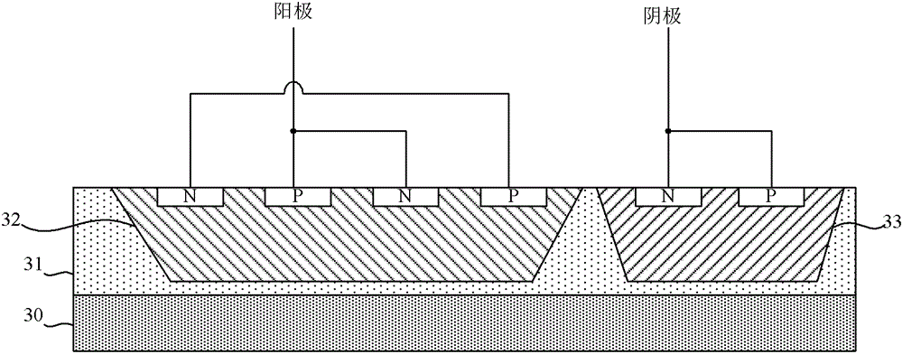
[0028] Such as image 3 As shown, a kind of SOI high sustain voltage thyristor device made by using the method for increasing the sustain voltage provided by the present invention includes: 30 is a buried oxide layer, and the material is silicon dioxide; 31 is a top oxide layer, which is used to make an SOI device main area of . In this example, an N well 32 and a P well 33 are formed in the P-type doped top oxide layer 31 with appropriate concentrations. As shown in the figure, P-type or N-type impurities are injected to form a high-concentration P+ region or a high-concentration N+ region, and an SOI thyristor device with a PNPN parasitic structure is formed between the anode and the cathode. As shown in the figure, a high sustaining voltage silicon controlled rectifier embedded in a diode or diode string can be made, and the diode or diode string can suppress positive feedback between parasitic PNP and NPN transistors, and increase the holding voltage of the silicon cont...
PUM
 Abstract
Description
Claims
Application Information
 - R&D Engineer
- R&D Manager
- IP Professional
- Industry Leading Data Capabilities
- Powerful AI technology
- Patent DNA Extraction
Browse by: Latest US Patents, China's latest patents, Technical Efficacy Thesaurus, Application Domain, Technology Topic, Popular Technical Reports.
© 2024 PatSnap. All rights reserved.Legal|Privacy policy|Modern Slavery Act Transparency Statement|Sitemap|About US| Contact US: help@patsnap.com