
Rubber conducting plate with multi-layer structure and conducting particles

A multi-layer structure, conductive plate technology, applied in the direction of rubber layered products, layered products, metal layered products, etc., can solve the problems of blocking conductive lines, wrong conduction, deformation and protrusion, etc., to prevent pollution, Clear function and shortened service life

Active Publication Date: 2012-06-20
NANTONG MEMTECH TECH
View PDF6 Cites 14 Cited by
  • Summary
  • Abstract
  • Description
  • Claims
  • Application Information

AI Technical Summary

Problems solved by technology

However, due to the thin metal surface layer, during long-term use, the rubber matrix is ​​easy to deform and protrude to the outside of the metal surface layer when it is pressed heavily or absorbs oil and expands, which may block the conductive line or even cause it to fail. or false turn-on condition

Method used

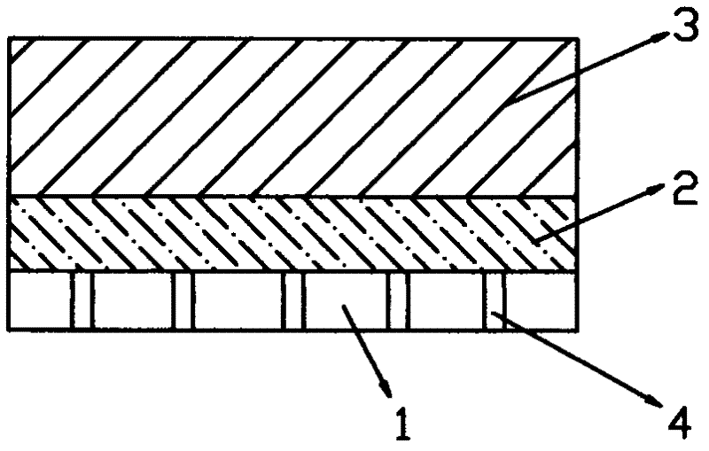

Image

  • Rubber conducting plate with multi-layer structure and conducting particles
  • Rubber conducting plate with multi-layer structure and conducting particles
  • Rubber conducting plate with multi-layer structure and conducting particles

Examples


Embodiment 1

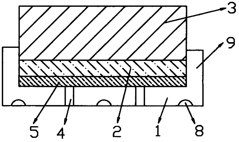
[0025] Embodiment 1: as figure 2 The rubber conductive particle with a multi-layer structure shown is composed of a conductive layer 1 , a transition layer 2 and an elastic layer 3 bonded together. The conductive layer 1 is a smooth dense metal silver sheet, the transition layer 2 is a composite sheet made of polyester film and a second layer of dense metal sheet 5 made of stainless steel, and the elastic layer 3 is a rubber sheet. The thickness of the conductive layer 1 is 0.05mm, the thickness of the transition layer 2 is 0.1mm, and the thickness of the elastic layer 3 is 2mm.

[0026] There are many randomly arranged holes 4 and a small number of dents 8 on the dense metal sheet of the conductive layer 1, and the maximum diameter of the holes 4 is less than 2 mm. The edge of the conductive layer 1 includes a flange 9 that bends toward the transition layer 2 and surrounds the transition layer, so as to further ensure that the elastic layer 3 will not be exposed from the pe...

Embodiment 2

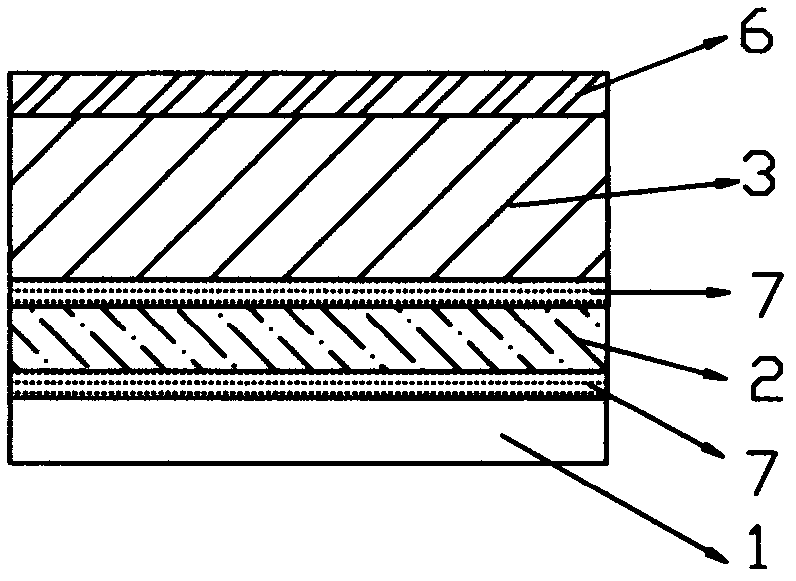
[0028] Embodiment 2: as image 3 The rubber conductive plate with multi-layer structure shown is composed of conductive layer 1, transition layer 2 and elastic layer 3 bonded and compounded. image 3 Among them, the conductive layer 1 is a mesh-shaped copper sheet; the transition layer 2 is a polyimide film; the elastic layer 3 is a rubber-plastic sheet. The thickness of the conductive layer 1 is 0.1 mm, the thickness of the transition layer 2 is 0.5 mm, and the thickness of the elastic layer 3 is 3 mm. A polymer adhesive layer 7 is formed between the conductive layer 1 and the transition layer 2 , and between the transition layer 2 and the elastic layer 3 . The outer surface of the elastic layer 3 also has a second polymer film 6 isolation layer. This embodiment is suitable for use as a conductive material or as an electromagnetic shielding material.

Embodiment 3

[0029] Embodiment 3: as figure 1 The rubber conductive plate shown is composed of a conductive layer 1 , a transition layer 2 and an elastic layer 3 . The conductive layer 1 is a metal plating layer, the transition layer 2 is a polycarbonate film; the elastic layer 3 is a rubber layer made of liquid silicone rubber. A 0.125mm thick polycarbonate film is used as the transition layer 2, and the surface is first plated with 0.5μm thick metal nickel and then 0.025μm thick gold by vacuum sputtering coating method. The plating layer forms the conductive layer 1 . Before vacuum sputtering nickel plating, the polycarbonate film is treated with plasma in a vacuum sputtering chamber, which can improve the adhesion between the metal nickel layer and the polycarbonate film. Coat one side of the polycarbonate film without metal plating with a primer that improves the adhesion between polycarbonate and silicone rubber, and then mold the liquid silicone rubber on the polycarbonate film at ...


PUM

PropertyMeasurementUnit
thicknessaaaaaaaaaa
thicknessaaaaaaaaaa
pore sizeaaaaaaaaaa

Abstract

The invention discloses a rubber conducting plate with a multi-layer structure and conducting particles. The rubber conducting plate with the multi-layer structure is formed by compositing a conducting layer, a transition layer and an elastic layer. Adhesive layers are arranged among the conducting layer, the transition layer and the elastic layer. The conducting layer is a compact metal thin sheet or a loose metal thin sheet. The transition layer is a polymer thin film or a second-layer compact metal thin sheet. The elastic layer is a rubber sheet or a rubber-plastic sheet, and the edge of the conducting layer can be provided with a turnup bending towards the direction of the transition layer and wrapping the transition layer. The conducting layer is made of metal with good conducting performance including gold, silver, copper, aluminum, iron and the like or alloy preferably. The metal thin sheet in transition layer is made of cheap metal including copper, iron, nickel, zinc, aluminum and the like and the alloy preferably. The conducting layer, the transition layer and the elastic layer of the rubber conducting plate with the multi-layer structure are tightly arranged together in compositing mode so as to have excellent specific strength. The conducting layer is completely separated from the elastic layer so that conducting capacity of the conducting layer is enhanced, and the elastic layer is prevented from protruding out of the conducting layer and influencing conducting effects. The rubber conducting plate with the multi-layer structure and conducting particles are applied to serve as conducting materials, electromagnetic shielding materials or conducting parts of a key.

Description

technical field [0001] The invention relates to a composite conductive rubber, which can be used for making conductive plates and conductive grains of key backings. Background technique [0002] Common rubber conductive plates or conductive particles are composed of a rubber base layer and a metal conductive surface layer. One side of the conductive plate has conductive properties, and the other side is insulated, which can be used as a conductive contact material or electromagnetic shielding material; the conductive particle is a conductive plate with a small area, which can be used as a conductive part for the backing of buttons. [0003] The applicant’s application number is 201110193369.5, which discloses a type of conductive particle composed of a metal surface layer and a rubber matrix, and the metal surface layer can form a relatively good contact with the circuit. . However, due to the thin metal surface layer, during long-term use, the rubber substrate is easily d...

Claims


Application Information

Patent Timeline
Patent Type & Authority Applications(China)
IPC IPC(8): B32B15/04B32B25/04B32B25/20
Inventor 黄诚黄志宏张劲松刘小平韩辉升
Owner NANTONG MEMTECH TECH
Learn More