Wafer processing sheet

A technology for thin sheet and wafer processing, which is applied in thin material processing, electrical components, circuits, etc., and can solve problems such as no existing known technology.

Active Publication Date: 2012-05-16
LG CHEM LTD
View PDF5 Cites 4 Cited by
  • Summary
  • Abstract
  • Description
  • Claims
  • Application Information

AI Technical Summary

Problems solved by technology

[0008] However, there is no prior known technology (including the above-mentioned Patent Document 1) for a sheet for handling wafers satisfying all the above-mentioned properties.

Method used


Image

  • Wafer processing sheet
  • Wafer processing sheet
  • Wafer processing sheet

Examples


Embodiment 1

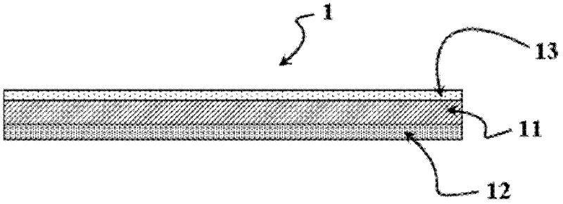
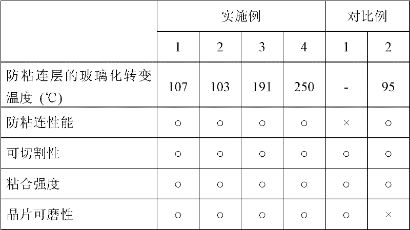
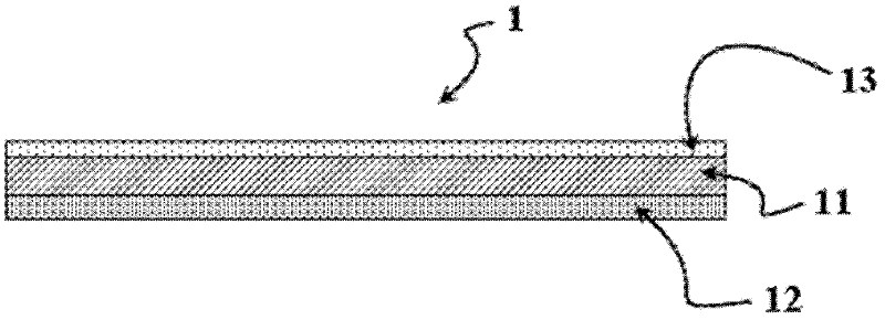
[0083] Formation of the anti-adhesion layer

[0084] A monomer mixture of 90 parts by weight of methyl methacrylate (MMA) and 10 parts by weight of hydroxyethyl methacrylate (HEMA) was polymerized to prepare an acrylic polymer having a solid content of 20 wt%. Subsequently, 10 parts by weight of an isocyanate curing agent (TDI) was mixed with the above-mentioned acrylic polymer with respect to 100 parts by weight of the above-prepared acrylic polymer to prepare a coating solution. Then, the above-prepared coating solution was coated on a polyester release film using a bar coater to have a thickness of 2 μm after drying; the coating layer was dried and aged under appropriate conditions to form Anti-blocking layer.

[0085] substrate formation

[0086] A monomer mixture comprising 70 parts by weight of 2-ethylhexyl acrylate (2-EHA), 27 parts by weight of isobornyl acrylate (IBOA) and 3 parts by weight of 2-hydroxyethyl acrylate (2-HEA) was put into the Reflux the 1L conta...

Embodiment 2

[0090]Wafers were processed according to the same method as described in Example 1, except that an isocyanate curing agent (TDI) was not used when forming the anti-blocking layer to form an anti-blocking layer comprising uncured acrylic polymer. to form.

Embodiment 3

[0092] In addition to using cellulose acetate resin instead of a mixture comprising an acrylic polymer and an isocyanate curing agent when forming the anti-blocking layer to form an anti-blocking layer comprising uncured cellulose acetate resin, the sheet for processing the wafer according to the The same method as described in Example 1 was formed.


PUM


Abstract

The present invention relates to a wafer processing sheet. The present invention provides a wafer processing sheet which is excellent in heat resistance and dimensional stability, and which has superior stress relaxation property to prevent a wafer from being damaged or delimited by residual stresses or a non-uniform pressure, and which has superior cutting property. In addition, the present invention provides a sheet which can effectively suppress a blocking phenomenon during a wafer processing process or the like. Consequently, a base of the present invention can be valuably used as a processing sheet in a variety of wafer processing processes including dicing, back grinding, picking-up and so on.

Description

technical field [0001] The invention relates to a wafer for handling wafers. Background technique [0002] A manufacturing method for a semiconductor device comprising a backgrinding process or a dicing process in which a sheet such as a surface protection sheet or a dicing sheet is used. [0003] In recent years, as the demand for dense and light-weight semiconductor devices has increased, the properties of such wafers for handling wafers have correspondingly become more important. [0004] For example, in order to manufacture circuits with a higher degree of integration than conventional methods (circuits are formed on only one side of the wafer), circuits should be formed on both sides of the wafer. In order to form circuits on both sides of the wafer, the wafer to which the processing sheet is attached should be subjected to high temperature treatment. Therefore, sheets used for handling wafers are required to have excellent heat resistance or dimensional stability at ...

Claims


Application Information

Patent Timeline
Patent Type & Authority Applications(China)
IPC IPC(8): H01L21/302
CPCH01L21/6836H01L2221/6834H01L2221/68327C09J2203/326C09J2433/006Y10T428/265Y10T428/31935Y10T428/31551Y10T428/31511C09J2301/162H01L21/30
Inventor 金世罗朱孝叔张锡基沈廷燮
Owner LG CHEM LTD
Why Eureka
Try Eureka