Method for manufacturing special-shaped chip through laser cutting
A technology of laser cutting and manufacturing methods, which is applied in manufacturing tools, laser welding equipment, semiconductor/solid-state device manufacturing, etc., can solve the problems of triangular chips with no use value and material waste, and achieve fast, efficient and simple processing, no material waste, The effect of high processing efficiency
- Summary
- Abstract
- Description
- Claims
- Application Information
AI Technical Summary
Problems solved by technology
Method used
Image

Examples
Embodiment 1
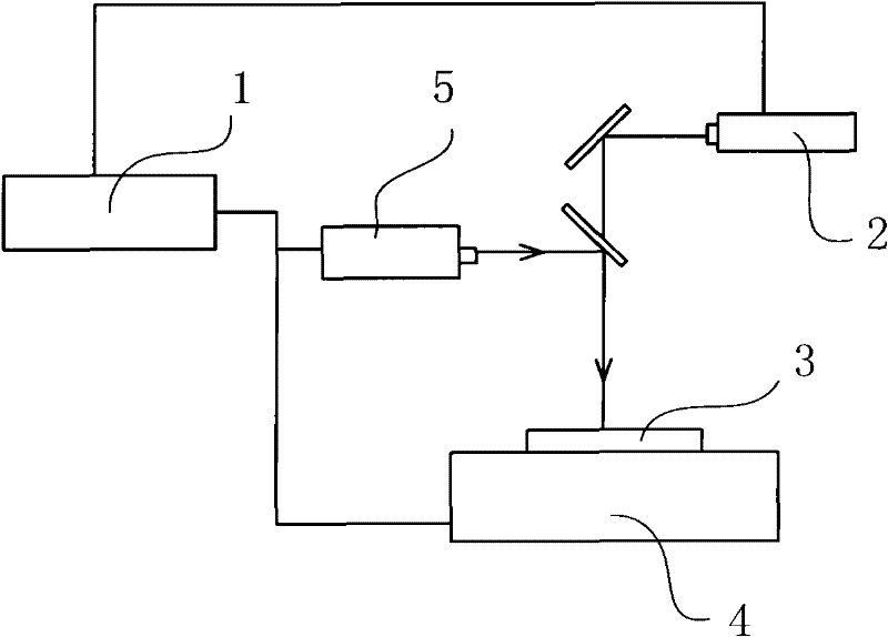
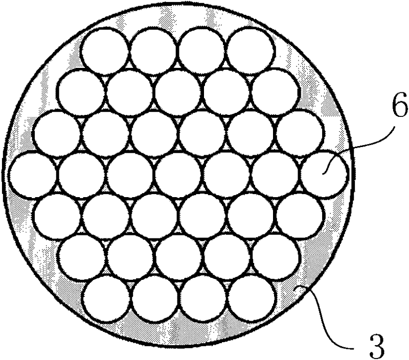
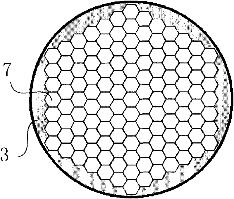
[0036] Fix the GPP semiconductor silicon wafer 3 with a circular glass passivation chip pattern on the semiconductor silicon wafer 3 on the workbench 4 through a vacuum chuck. Then, the charge-coupled device image sensor 2 device assists positioning, and the laser beam emitted by the gas laser 5 is used to irradiate the semiconductor wafer vertically, and the operation of the workbench 4 is controlled by software.
[0037] Specifically, the operator can set wafer parameters on the control software, including the size and diameter of the special-shaped wafer to be obtained. At the same time, the parameters of the laser beam can be set, including laser power, laser frequency, and laser pulse width. Moreover, the motion control parameters of the workbench 4 can also be set, including scribing speed, acceleration, deceleration and so on. Once, the workbench 4 is made to move relative to the laser beam according to the circular glass passivation chip pattern on the semiconductor s...
Embodiment 2
[0041] Fix the GPP semiconductor silicon wafer 3 with a circular glass passivation chip pattern on the semiconductor silicon wafer 3 on the workbench 4 through a vacuum chuck. Then, the charge-coupled device image sensor 2 device assists positioning, and the laser beam emitted by the semiconductor laser is used to irradiate the semiconductor wafer vertically, and the operation of the workbench 4 is controlled by software.
[0042]Specifically, the operator can set wafer parameters on the control software, including the size and diameter of the special-shaped wafer to be obtained. At the same time, the parameters of the laser beam can be set, including laser power, laser frequency, and laser pulse width. Moreover, the motion control parameters of the workbench 4 can also be set, including scribing speed, acceleration, deceleration and so on. Once, the workbench 4 is made to move relative to the laser beam according to the circular glass passivation chip pattern on the semicond...
Embodiment 3
[0046] Fix the GPP semiconductor silicon wafer 3 with a circular glass passivation chip pattern on the semiconductor silicon wafer 3 on the workbench 4 through a vacuum chuck. Then, the charge-coupled device image sensor 2 device assists in positioning, and the laser beam emitted by the fiber laser is vertically irradiated on the semiconductor wafer, and the operation of the workbench 4 is controlled by software.
[0047] Specifically, the operator can set wafer parameters on the control software, including the size and diameter of the special-shaped wafer to be obtained. At the same time, the parameters of the laser beam can be set, including laser power, laser frequency, and laser pulse width. Moreover, the motion control parameters of the workbench 4 can also be set, including scribing speed, acceleration, deceleration and so on. Once, the workbench 4 is made to move relative to the laser beam according to the circular glass passivation chip pattern on the semiconductor si...
PUM
| Property | Measurement | Unit |
|---|---|---|
| Wavelength | aaaaa | aaaaa |
Abstract
Description
Claims
Application Information
 - R&D
- Intellectual Property
- Life Sciences
- Materials
- Tech Scout
- Unparalleled Data Quality
- Higher Quality Content
- 60% Fewer Hallucinations
Browse by: Latest US Patents, China's latest patents, Technical Efficacy Thesaurus, Application Domain, Technology Topic, Popular Technical Reports.
© 2025 PatSnap. All rights reserved.Legal|Privacy policy|Modern Slavery Act Transparency Statement|Sitemap|About US| Contact US: help@patsnap.com