Preparation method and application of nanoimprint template
A technology of nanoimprinting and stencil, which is applied in the field of preparation of nanowires or nanotubes and templates for nanoimprinting, which can solve the problem of affecting the quality of nanostructures, increasing product costs, and reducing the stability of nanostructures. and performance reliability issues, to achieve the effect of reducing the preparation cost and instrument price
- Summary
- Abstract
- Description
- Claims
- Application Information
AI Technical Summary
Problems solved by technology
Method used
Image
Examples
Embodiment 1
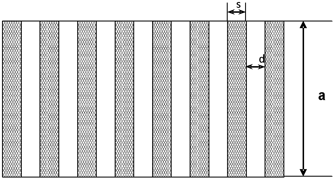
[0057] Porous nano-alumina template A is used, and the specific size of the template A is as follows: the substrate is aluminum with a thickness c=1 μm; the shape of the nanohole is circular, the aperture size d=5nm, the hole spacing s=7.5nm, and the hole depth a is 10nm , The thickness of the barrier layer at the bottom of the hole b=1nm. The specific steps of using it to prepare a template for nanoimprinting are as follows:
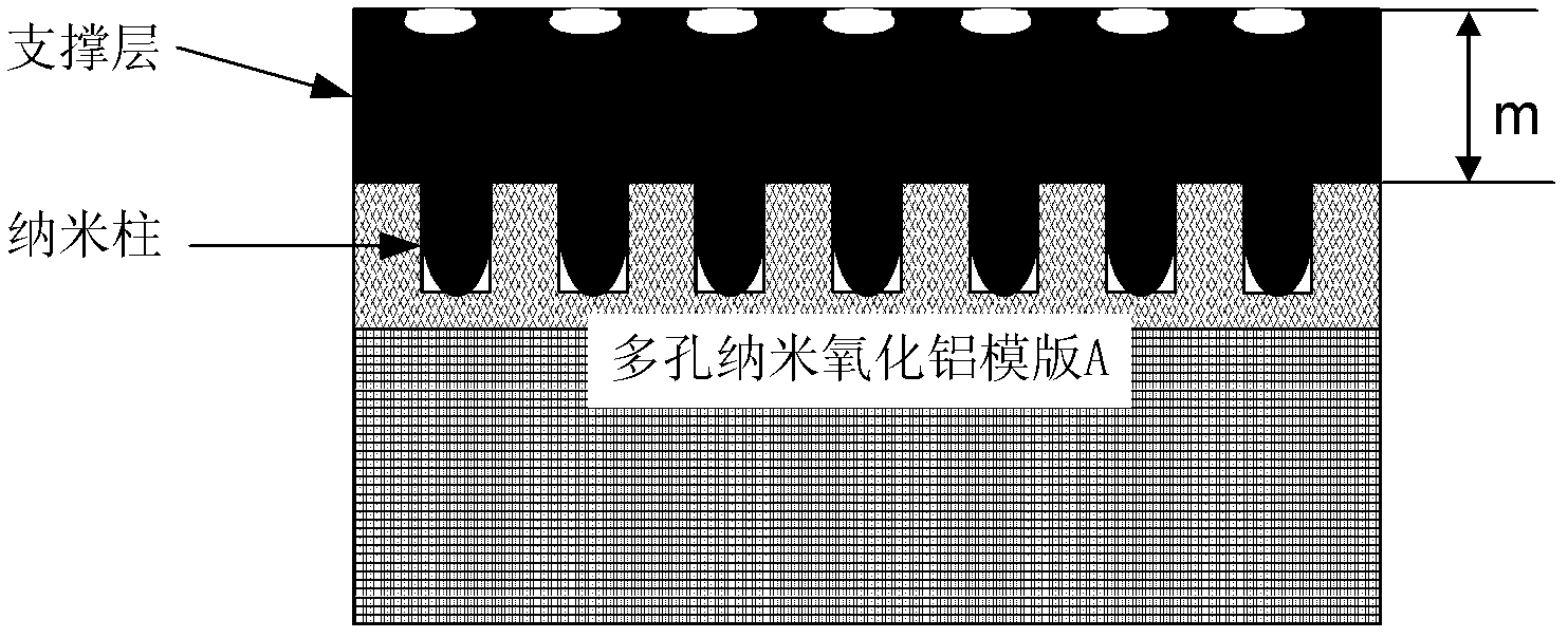
[0058] Step 1: Using the copper target as the filling material, deposit copper atoms into the pores of the porous nano-alumina template A by magnetron sputtering at a sputtering rate of 1nm / min, and fill it into a nanometer with a spherical or ellipsoidal head. The radius of curvature of the column, spherical or ellipsoidal head is 3 nanometers; continue to deposit a copper surface support layer with a thickness of 0.5 μm on the upper surface (opening direction) of the porous nano-alumina template A.
[0059] Step 2: Coating a copper transition layer w...
Embodiment 2
[0063] Porous nano-alumina is used as the template B, and the specific size of the template B is as follows: the shape of the nanopore is circular, the aperture size d=13nm, the hole spacing s=6.5nm, and the hole depth a=500nm. The specific steps of using it to prepare a template for nanoimprinting are as follows:
[0064] Step 1: By magnetron sputtering, using titanium as the target material, at a sputtering rate of 10nm / min, deposit titanium into the porous nano-alumina template B to form a nano-column with a ring-shaped head. The column height g is 100nm, the ring wall thickness t of the annular structure is 3 nanometers, and the depth h is 5nm; continue to deposit on the upper surface (opening direction) of the porous nano-alumina template B to form a titanium surface support layer with a thickness m of 1 μm .
[0065] Step 2: On another quartz substrate with a thickness of 1 mm, a titanium transition layer with a thickness of about 10 nm is coated with the same material ...
Embodiment 3
[0069] GaAs nanowires were prepared on a silicon substrate by using the template for nanoimprinting with a nanocolumn structure diameter of 5 nm and a height of 10 nm prepared in Example 1. The specific steps are as follows: first, the silicon substrate is washed with 30% HF solution, rinsed with ultrapure water, and dried with argon. Then rotate the surface at 5000 revolutions per minute (rpm) for 30 seconds, spin-coat a layer of photosensitive resin (Shipley 1813) with a thickness of 10-15 nanometers, and bake at 80°C for 10-30 seconds to make it semi-cured. Next, the stencil for nanoimprint prepared in Example 1 was placed on it, and 20 N / cm 2 Then, after baking at 110°C for 60 seconds, the template for nanoimprinting was removed, and then baked at 110°C for 60 seconds to fully cure. Afterwards, it was placed in a reactive ion beam cleaner at 100°C with 20 sccm (cm 3 / min, at 20°C and 1 atmosphere) the oxygen plasma flow will wash the residual resin at the bottom of the p...
PUM
| Property | Measurement | Unit |
|---|---|---|
| thickness | aaaaa | aaaaa |
| thickness | aaaaa | aaaaa |
| thickness | aaaaa | aaaaa |
Abstract
Description
Claims
Application Information
 - R&D Engineer
- R&D Manager
- IP Professional
- Industry Leading Data Capabilities
- Powerful AI technology
- Patent DNA Extraction
Browse by: Latest US Patents, China's latest patents, Technical Efficacy Thesaurus, Application Domain, Technology Topic, Popular Technical Reports.
© 2024 PatSnap. All rights reserved.Legal|Privacy policy|Modern Slavery Act Transparency Statement|Sitemap|About US| Contact US: help@patsnap.com


