Anti-welding adhesive tape

A tape and anti-soldering technology, applied in the direction of adhesives, film/sheet adhesives, layered products, etc., can solve the problems of scrapped printed circuit boards, exposed small holes of printed circuit boards, prone to shrinkage and falling off, etc. Achieve good tearability

Inactive Publication Date: 2012-04-04
常熟市富邦胶带有限责任公司
View PDF2 Cites 2 Cited by
  • Summary
  • Abstract
  • Description
  • Claims
  • Application Information

AI Technical Summary

Problems solved by technology

The existing solder resist tape is formed by coating a pressure-sensitive layer on the substrate film layer. The tape substrate of this structure is a single-layer structure. This type of tape is used to adhere to the small holes of the printed circuit board as a shielding protection. And when the printed circuit board is sent to the wave soldering furnace, it is prone to shrinkage and shedding, which will cause the small holes on the printed circuit board to be exposed, resulting in the scrapping of the printed circuit board

Method used


Image

  • Anti-welding adhesive tape
  • Anti-welding adhesive tape

Examples


Embodiment Construction

[0012] The preferred embodiments of the present invention will be described in detail below with reference to the accompanying drawings, so that the advantages and features of the present invention can be more easily understood by those skilled in the art, so as to make a clearer and clearer definition of the protection scope of the present invention.

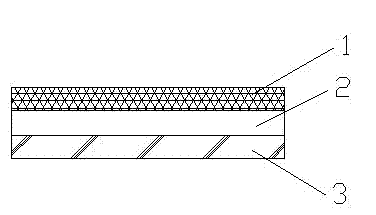
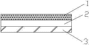
[0013] See figure 1 As shown, the embodiment of the present invention includes:

[0014] A solder mask tape, comprising a substrate film layer 2, a reinforcing tape 3 and a pressure-sensitive layer 1, wherein the reinforcing tape 3 is coated on one side surface of the substrate film layer 2, and the pressure-sensitive The layer 1 is coated on the other side surface of the base film layer 2.

[0015] The base film layer 2 is a polyimide film layer, which has outstanding high temperature resistance, radiation resistance, chemical corrosion resistance and electrical insulation properties, and can be used for a long time in the air at 25...


PUM


Abstract

The invention discloses an anti-welding adhesive tape. The anti-welding adhesive tape comprises a base material film layer, a reinforcing belt and a pressure-sensitive layer and is characterized in that: the reinforcing belt is coated on the surface of one side of the base material film layer; and the pressure-sensitive layer is coated on the surface of the other side of the base material film layer. The base material film layer is combined with the reinforcing belt structure, so that the original single-layer base material structure is changed into a double-layer composite structure, and the anti-welding adhesive tape has ideal high temperature resistance, is not shrunk and deformed during use at high temperature, is soft and comfortable and has high tearability.

Description

Technical field [0001] The invention relates to the technical field of manufacturing and application of electronic products and their components, in particular to a solder mask tape. Background technique [0002] At present, in the object processing process of high-temperature engineering in the field of electronic product manufacturing, various tapes are needed to protect the shielding parts. For example, in the process of sending the printed circuit board into the tin furnace for wave soldering, it is necessary to use solder mask The small holes on the printed circuit board are blocked and protected. The existing solder mask tape is formed by coating a pressure-sensitive layer on a substrate film layer. The tape substrate of this structure has a single-layer structure. This type of tape is used to adhere to the small holes of the printed circuit board as a shielding protection. When the printed circuit board is sent to the tin furnace for wave soldering, it is prone to shrinka...

Claims


Application Information

Patent Timeline
IPC IPC(8): C09J7/02C09J183/04B32B27/10B32B27/28
Inventor 沈加平
Owner 常熟市富邦胶带有限责任公司
Why Eureka
Try Eureka