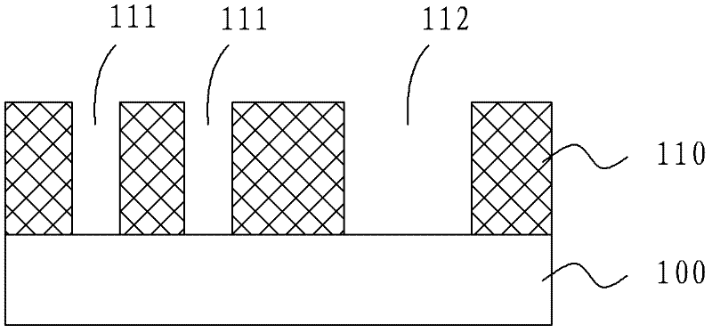
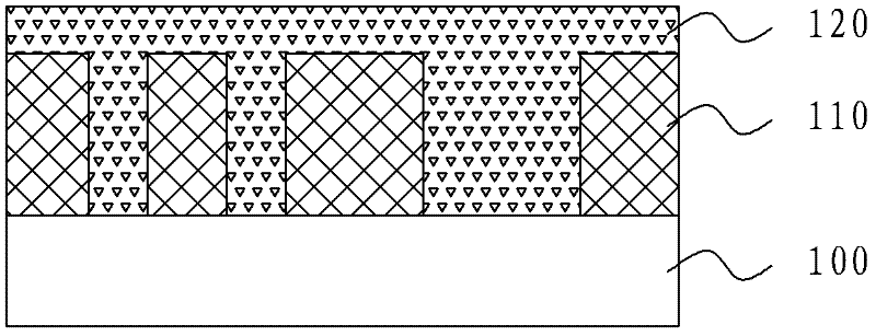
Method for manufacturing damascene structure
A manufacturing method and a technology of a dielectric layer, applied in semiconductor/solid-state device manufacturing, electrical components, circuits, etc., can solve problems affecting the electrical performance of metal wires 121, the speed of current passing through metal wires 121, and the speed of chips, etc.
- Summary
- Abstract
- Description
- Claims
- Application Information
AI Technical Summary
Problems solved by technology
Method used
Image
Examples
Embodiment Construction
[0024] The present invention is described in detail below in conjunction with accompanying drawing:
[0025] Please refer to figure 2 , the Damas structure manufacturing method of the present invention, comprises the following steps:
[0026] First, execute step S201, please refer to Figure 3A , forming a first dielectric layer 310 on the semiconductor substrate 300, wherein the material of the first dielectric layer 310 is, for example, silicon dioxide. As a preferred implementation mode, the material of the first dielectric layer adopts the trade name of Black diamond (Black Diamond, BD) silicon carbide or carbon-doped silicon oxide;
[0027] Then, execute step S202, please refer to Figure 3B , forming a metal wire groove 311 and a redundant metal wire groove 312 in the first dielectric layer 310, the metal wire groove 311 exposes the semiconductor substrate 310, and the depth of the redundant metal wire groove 312 can be equal to that of the metal wire The grooves 31...
PUM
 Abstract
Description
Claims
Application Information
 - Generate Ideas
- Intellectual Property
- Life Sciences
- Materials
- Tech Scout
- Unparalleled Data Quality
- Higher Quality Content
- 60% Fewer Hallucinations
Browse by: Latest US Patents, China's latest patents, Technical Efficacy Thesaurus, Application Domain, Technology Topic, Popular Technical Reports.
© 2025 PatSnap. All rights reserved.Legal|Privacy policy|Modern Slavery Act Transparency Statement|Sitemap|About US| Contact US: help@patsnap.com


