


Quick Research
Generate reliable direction feasibility study reports for your R&D in just a few steps.

Technical Q&A
Discover and master advanced knowledge NOW. Basics, ideas, possibilities, all at once.

Find Solutions
As an expert in R&D theories, this can generate solutions to your technical problems instantly.

Evaluate Feasibility
Analyze your overall solution with one click, know your potential R&D risks in advance.

Monitor Landscape
Get weekly tech updates, stay abreast of the latest tech innovations and key insights.
Preparation process for anti-oxidation copper-based bonding wires
A preparation process and bonding wire technology, which is applied in semiconductor/solid-state device manufacturing, electrical components, circuits, etc., can solve the problems of bonding wire packaging, high price of bonding gold wire and hardness of bonding copper wire, etc., to reduce impact force and Effects of destroying, reducing bonding energy, and improving hardness
- Summary
- Abstract
- Description
- Claims
- Application Information
AI Technical Summary
Problems solved by technology
Method used
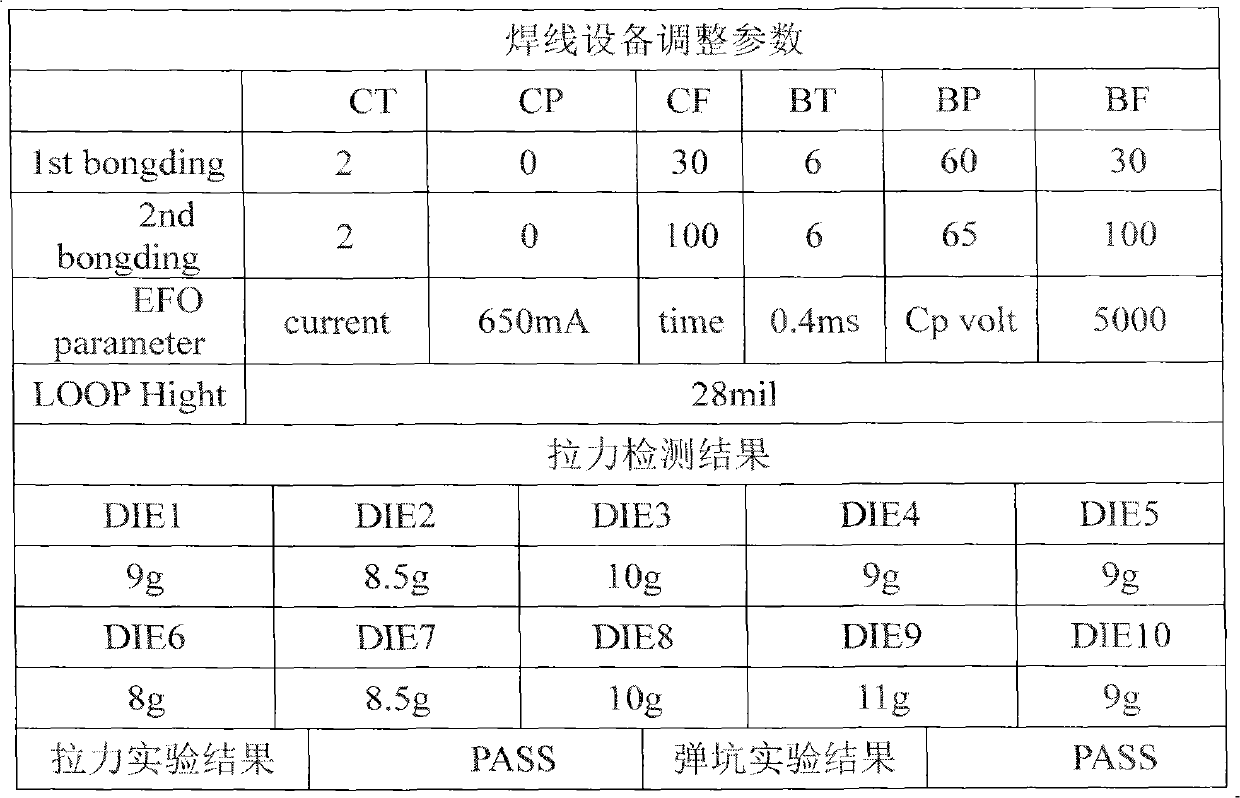
Image

Examples
Embodiment 1
[0028] A copper-based bonding wire, the basic material is copper, and Pt, Ce, Pd trace metal elements are added to form a master alloy base material, and the surface of the metal wire made of the master alloy base material is plated with a layer of gold. Among them, the purity of copper and plated gold are higher than 99.99%.
[0029] The weight proportion of each metal component in the bonding wire material is: Cu is 94.9933%, trace metal element Pt is 0.0007%, Ce is 0.002%, Pd is 0.004%, plated gold is 5%, and the diameter of the bonding wire is 50 microns , the gold layer thickness is 0.6 μm.
[0030] The preparation of copper-based bonding wire includes the following steps:
[0031] The first step is to mix the metal substrate. Cu with a purity higher than 99.99% is mixed with selected trace metal materials Pt, Ce, and Pd to form the base alloy of the master alloy, and the preliminary preparation for mixed smelting is done.
[0032] Step 2, smelting the mother alloy bla...
Embodiment 2
[0040]A copper-based bonding wire, the basic material is copper, and Pt, Ce, Pd trace metal elements are added to form a master alloy base material, and the surface of the metal wire made of the master alloy base material is plated with a layer of gold. Among them, the purity of copper and plated gold are higher than 99.99%.
[0041] The mass proportion of each metal component in the bonding wire material is: Cu is 95.9923%, trace metal element Pt is 0.0007%, Ce is 0.004%, Pd is 0.003%, gold plating is 4% gold, and the diameter of the bonding wire is 50% microns, with a gold layer thickness of 0.5 microns.
[0042] The preparation process of the copper-based bonding wire includes the following steps:
[0043] The first step is to mix the metal substrate. Cu with a purity higher than 99.99% is mixed with selected trace metal materials Pt, Ce, and Pd to form the base alloy of the master alloy, and the preliminary preparation for mixed smelting is done.
[0044] Step 2, smelti...
PUM
| Property | Measurement | Unit |
|---|---|---|
| diameter | aaaaa | aaaaa |
Abstract
Description
Claims
Application Information
 - R&D Engineer
- R&D Manager
- IP Professional
- Industry Leading Data Capabilities
- Powerful AI technology
- Patent DNA Extraction
Browse by: Latest US Patents, China's latest patents, Technical Efficacy Thesaurus, Application Domain, Technology Topic, Popular Technical Reports.
© 2024 PatSnap. All rights reserved.Legal|Privacy policy|Modern Slavery Act Transparency Statement|Sitemap|About US| Contact US: help@patsnap.com