N-type doped zns quasi-one-dimensional nanostructure film photoconductive ultraviolet detector and preparation method
An ultraviolet detector and nanostructure technology, applied in nanotechnology, nanotechnology, semiconductor devices, etc., can solve the problems of low response speed, small responsivity, and difficult application of UV detectors, and improve the responsivity and sensitivity of ultraviolet light. High and low cost effect
- Summary
- Abstract
- Description
- Claims
- Application Information
AI Technical Summary
Problems solved by technology
Method used
Image
Examples
Embodiment 1
[0029] The preparation method and steps of Cl-doped ZnS nanowire film photoconductive ultraviolet detector are as follows:
[0030] 1. After ultrasonically cleaning the silicon wafer with a thickness of 300nm silicon oxide on the surface, use alcohol as the dispersion liquid, and synthesize the doping concentration by chemical vapor phase method to 2.6×10 16 cm -3 The Cl-doped ZnS nanowires were added into the dispersion liquid, and the nanowires were evenly suspended in the dispersion liquid by ultrasonic vibration.
[0031] 2. Spin-coat the dispersion containing ZnS nanobelts on a clean silicon wafer with silicon oxide, and form a ZnS nanobelt film through volatilization.
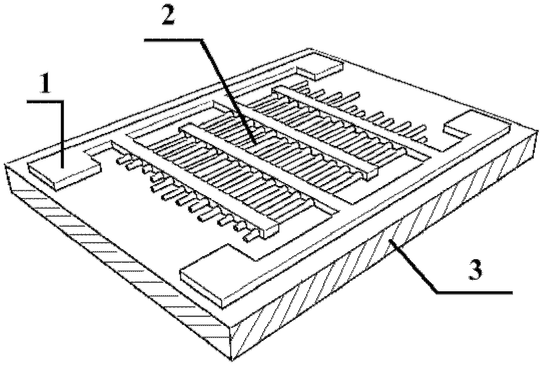
[0032] 3. Spin-coat photoresist on the silicon wafer coated with the ZnS nanowire film, and photo-etch the interdigital electrode 2 pattern, the distance between adjacent interdigital electrodes is 5 μm, and the width is 10 μm.
[0033] 4. Prepare a layer of AZO electrode with a thickness of 50 nm on th...
Embodiment 2
[0037] The preparation method and steps of Ga-doped ZnS nanobelt film photoconductive ultraviolet detector are as follows:
[0038] 1. After the quartz glass is ultrasonically cleaned, acetone is used as the dispersion liquid, and the doping concentration of the chemical vapor phase synthesis is 1.5×10 17 cm -3 The Ga-doped ZnS nanobelts are added into the dispersion liquid, and the nanobelts are evenly suspended in the dispersion liquid by ultrasonic vibration.
[0039] 2. Spin-coat the dispersion containing ZnS nanobelts on the quartz glass, and form a ZnS nanobelt film through volatilization;
[0040] 3. Spin-coat photoresist on the quartz glass coated with ZnS nanobelt film, and photo-etch the pattern of interdigitated electrodes. The distance between adjacent electrodes of the interdigitated electrodes is 10 μm, and the width is 100 μm;
[0041] 4. Prepare a layer of ITO electrode on the photolithographic electrode by pulse laser deposition method, with a thickness of 2...
Embodiment 3
[0044] The preparation method and steps of Al-doped ZnS nanowire film photoconductive ultraviolet detector are as follows:
[0045] 1. After ultrasonically cleaning the silicon wafer coated with silicon nitride with a thickness of 50nm on the surface, use alcohol as the dispersion liquid, and the doping concentration of the chemical vapor phase synthesis is 3.8×10 17 cm -3The Al-doped ZnS nanowires are added to the dispersion liquid, and the nanowires are evenly suspended in the dispersion liquid by ultrasonic vibration;
[0046] 2. Spin-coat the dispersion containing ZnS nanowires on a clean silicon wafer coated with silicon nitride, and form a ZnS nanowire film through volatilization;
[0047] 3. Spin-coat photoresist on the silicon wafer coated with ZnS nanowire film, and photo-etch the pattern of interdigitated electrodes. The distance between adjacent electrodes of the interdigitated electrodes is 50 μm, and the width is 50 μm;
[0048] 4. Prepare a layer of AZO electro...
PUM
| Property | Measurement | Unit |
|---|---|---|
| Width | aaaaa | aaaaa |
| Thickness | aaaaa | aaaaa |
| Thickness | aaaaa | aaaaa |
Abstract
Description
Claims
Application Information
 - Generate Ideas
- Intellectual Property
- Life Sciences
- Materials
- Tech Scout
- Unparalleled Data Quality
- Higher Quality Content
- 60% Fewer Hallucinations
Browse by: Latest US Patents, China's latest patents, Technical Efficacy Thesaurus, Application Domain, Technology Topic, Popular Technical Reports.
© 2025 PatSnap. All rights reserved.Legal|Privacy policy|Modern Slavery Act Transparency Statement|Sitemap|About US| Contact US: help@patsnap.com


