Method for preparing magnesium diboride superconducting thin film by electron beam annealing
A technology of electron beam annealing and magnesium diboride, which is applied in the manufacture/processing of superconductor devices, can solve the problems of unfavorable high-quality superconducting thin films, high Mg vapor pressure, and formation of impurities, and achieve high annealing efficiency and heating and cooling speed Fast and reduce the effect of volatilization
- Summary
- Abstract
- Description
- Claims
- Application Information
AI Technical Summary
Problems solved by technology
Method used
Image
Examples
Embodiment 1
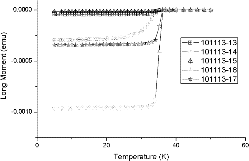
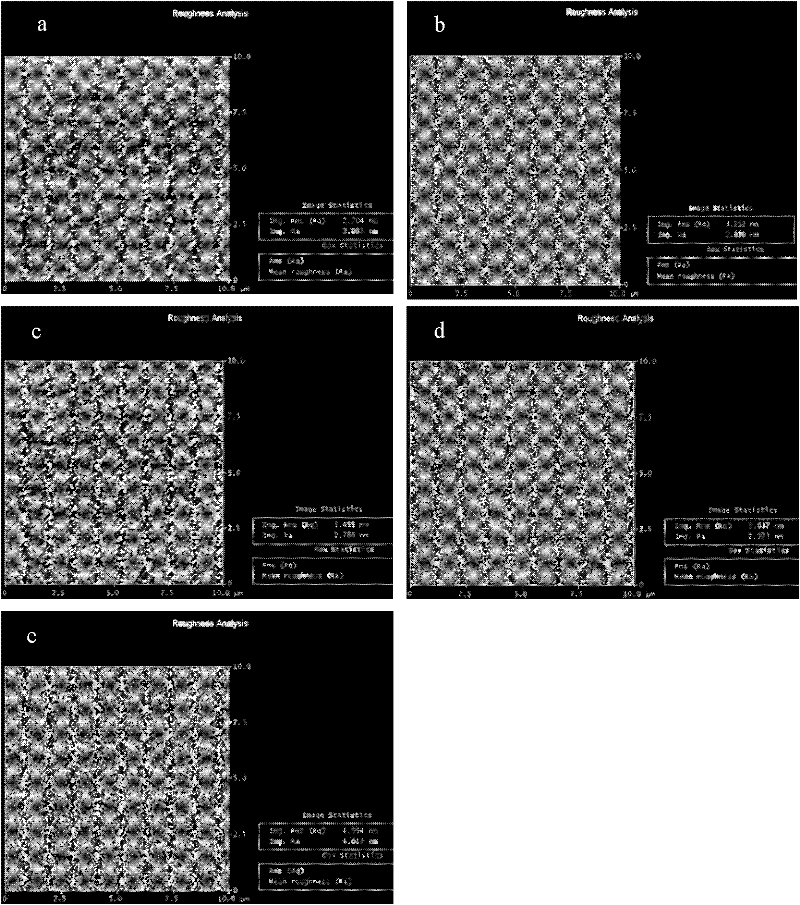
[0024] Electron beam annealing was carried out on a self-made EBW-6 electron beam welding machine. Pioneer film is That is, N=1, the film thickness is 20nm, the size of the precursor film is 10.0mm×3.0mm, and the substrate is SiC.
[0025] 1. Place the bare substrate SiC with the same size as the precursor film on the movable workpiece stage in the sample chamber of the electron beam processing equipment. When the vacuum degree of the sample chamber is higher than 1.0×10 -2 Pa, continue to operate as follows;
[0026] 2. According to the formula in step 2, the effective penetration depth R=23nm of the electrons accelerated by the 1kV voltage in the precursor film is obtained, which is greater than the thickness of the sample film of 20nm, so the electron beam acceleration voltage U=1kV is selected;
[0027] 3. Select beam current I and beam spot size Ф: load accelerating voltage U = 1kV, adjust electron beam current I, and adjust beam spot diameter Ф at the same time, when ...
Embodiment 2
[0031] Electron beam annealing was carried out on a self-made EBW-6 electron beam welding machine. Pioneer film is That is, N=5, the film thickness is 100 nm, the size of the precursor film is 10.0 mm×3.0 mm, and the substrate is SiC.
[0032] 1. Place the bare substrate SiC with the same size as the precursor film on the movable workpiece stage in the sample chamber of the electron beam processing equipment, and vacuum the sample chamber to a vacuum degree higher than 1.0×10 -2 Pa;
[0033]2. According to the formula in step 2, the effective penetration depth R=4394nm of the electrons accelerated by the 20kV voltage in the precursor film is obtained, which is greater than the thickness of the sample film of 100nm, so the electron beam acceleration voltage U=20kV is selected;
[0034] 3. Select I=16.0mA, Ф=12.0mm;
[0035] 4. Select the annealing time t=0.14s;
[0036] 5. Place the precursor film on the movable workpiece stage in the sample chamber of the electron beam pr...
Embodiment 3
[0038] Electron beam annealing was carried out on a self-made EBW-6 electron beam welding machine. Pioneer film is That is, N=5, the film thickness is 100 nm, the size of the precursor film is 10.0 mm×3.0 mm, and the substrate is Si.
[0039] 1. Place the bare substrate SiC with the same size as the precursor film on the movable workpiece stage in the sample chamber of the electron beam processing equipment, and vacuum the sample chamber to a vacuum degree higher than 1.0×10 -2 Pa;
[0040] 2. With embodiment two, select U=20kV;
[0041] 3. Select I=2.0mA, Ф=8.0mm;
[0042] 4. Select the annealing time t=0.32s;
[0043] 5. Put the precursor film on the movable workpiece stage in the sample chamber of the electron beam processing equipment, set U=20kV, I=2.0mA, Ф=8.0mm. Since the length of the precursor film is 10 mm greater than the diameter of the beam spot of 8 mm, the moving workpiece table is moved so that the precursor film passes directly under the beam spot at a u...
PUM
| Property | Measurement | Unit |
|---|---|---|
| Roughness | aaaaa | aaaaa |
| Transition temperature | aaaaa | aaaaa |
| Roughness | aaaaa | aaaaa |
Abstract
Description
Claims
Application Information
 - R&D
- Intellectual Property
- Life Sciences
- Materials
- Tech Scout
- Unparalleled Data Quality
- Higher Quality Content
- 60% Fewer Hallucinations
Browse by: Latest US Patents, China's latest patents, Technical Efficacy Thesaurus, Application Domain, Technology Topic, Popular Technical Reports.
© 2025 PatSnap. All rights reserved.Legal|Privacy policy|Modern Slavery Act Transparency Statement|Sitemap|About US| Contact US: help@patsnap.com


