


Quick Research
Generate reliable direction feasibility study reports for your R&D in just a few steps.

Technical Q&A
Discover and master advanced knowledge NOW. Basics, ideas, possibilities, all at once.

Find Solutions
As an expert in R&D theories, this can generate solutions to your technical problems instantly.

Evaluate Feasibility
Analyze your overall solution with one click, know your potential R&D risks in advance.

Monitor Landscape
Get weekly tech updates, stay abreast of the latest tech innovations and key insights.
Large-area organic thin film transistor array preparation method compatible with roll-to-roll technology
A large-area, organic film technology, used in semiconductor/solid-state device manufacturing, electrical solid-state devices, semiconductor devices, etc., can solve the problem of easy reaction and mutual mixing, unguaranteed interface quality, and difficulty in preparing large-area organic films with uniform thickness. Small molecule thin film and other problems, to achieve the effect of economical and efficient use of raw materials, uniform device performance, and excellent device indicators
- Summary
- Abstract
- Description
- Claims
- Application Information
AI Technical Summary
Problems solved by technology
Method used
Image

Examples
Embodiment 1
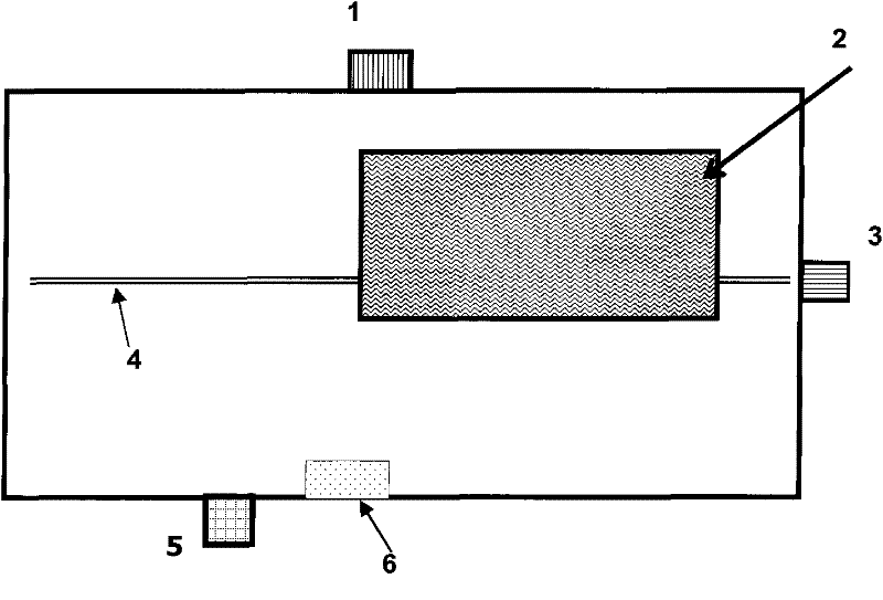
[0034] refer to image 3 In this embodiment, clean PET (polyethylene terephthalate) plated with ITO (indium tin oxide) is used as the substrate, and the substrate also serves as the gate electrode.
[0035] Prepare a polystyrene insulating dielectric layer on the gate electrode: spin-coat a polystyrene insulating dielectric layer (toluene solution, mass concentration 5%, rotating speed 2000rpm / min) on the upper surface of the substrate, and bake for 3 hours at 80°C , the thickness of the polystyrene insulating dielectric layer is about 500nm.
[0036] Fabrication of pentacene thin films on polystyrene insulating dielectric layers: using figure 1 In the vacuum coating system shown, the lower surface of the substrate prepared sequentially with the gate electrode and the polystyrene insulating dielectric layer is pasted on the roller, and the vacuum degree is 1.2×10 -3 Under the conditions of Pa and room temperature, pentacene was deposited on the polystyrene insulating dielect...
Embodiment 2
[0044] refer to image 3 In this embodiment, an n-type heavily doped silicon wafer is used as a substrate, and the substrate is used as a gate at the same time; the n-type heavily doped silicon wafer (substrate) is cut into 15 mm × 15 mm flake-like small pieces, and carried out cleaning;
[0045] Prepare an insulating dielectric layer on the upper surface of the n-type heavily doped silicon wafer substrate: spin-coat a polystyrene dielectric layer (toluene solution, mass concentration 5%, rotating speed 2000rpm / min) on the upper surface of the substrate, bake at 80 ° C Baking for 3 hours, the thickness of the polystyrene insulating dielectric layer is about 500nm.
[0046] Fabrication of Pentacene Films on Polystyrene Insulating Dielectric Layers: Using figure 1 In the vacuum coating system shown, the lower surface of the substrate prepared sequentially with the gate electrode and the polystyrene insulating dielectric layer is pasted on the roller, and the vacuum degree is 9...
Embodiment 3
[0054] refer to image 3 , first make a gate electrode on the upper surface of the substrate. In this embodiment, an n-type heavily doped silicon wafer is used as the substrate and at the same time as the gate; a silicon dioxide dielectric layer (using thermally oxidized silicon dioxide Dielectric layer, thickness 290nm).
[0055] The substrate prepared with the silicon dioxide insulating dielectric layer was cut into small pieces of 10mm×10mm, and the surface was cleaned.
[0056] The lower surface of the substrate prepared with a silicon dioxide insulating dielectric layer is pressed Figure 5 Way to paste on the roller; use figure 1 The vacuum coating system shown in the vacuum degree is 9×10 -4 Pa and room temperature conditions, use the vacuum thermal evaporation method to vapor-deposit hexathiophene on the silicon dioxide insulating dielectric layer for 70min, and prepare the hexathiophene film;
[0057] During the evaporation process of the hexathiophene film, the r...
PUM
| Property | Measurement | Unit |
|---|---|---|
| thickness | aaaaa | aaaaa |
| thickness | aaaaa | aaaaa |
| thickness | aaaaa | aaaaa |
Abstract
Description
Claims
Application Information
 - R&D Engineer
- R&D Manager
- IP Professional
- Industry Leading Data Capabilities
- Powerful AI technology
- Patent DNA Extraction
Browse by: Latest US Patents, China's latest patents, Technical Efficacy Thesaurus, Application Domain, Technology Topic, Popular Technical Reports.
© 2024 PatSnap. All rights reserved.Legal|Privacy policy|Modern Slavery Act Transparency Statement|Sitemap|About US| Contact US: help@patsnap.com