Method and system for manufacturing semiconductor

A manufacturing method, semiconductor technology, applied in the field of measurement models

Active Publication Date: 2011-09-28
TAIWAN SEMICON MFG CO LTD
View PDF7 Cites 3 Cited by
  • Summary
  • Abstract
  • Description
  • Claims
  • Application Information

AI Technical Summary

Problems solved by technology

[0004] Therefore, although the existing virtual measurement technology can meet the original purpose, it is not suitable for all aspects

Method used


Image

  • Method and system for manufacturing semiconductor
  • Method and system for manufacturing semiconductor
  • Method and system for manufacturing semiconductor

Examples


Embodiment Construction

[0034] It should be understood that the following descriptions are intended to provide various embodiments or examples to achieve different features of this specification. The following examples of specific components and arrangements are used to simplify the description. These embodiments are of course only examples and are not intended to be limiting. In addition, repeated numbers or letters may be used in different embodiments in the description of this specification. These repetitions are for simplification and clarification and are not intended to establish relationships between different embodiments and / or structures.

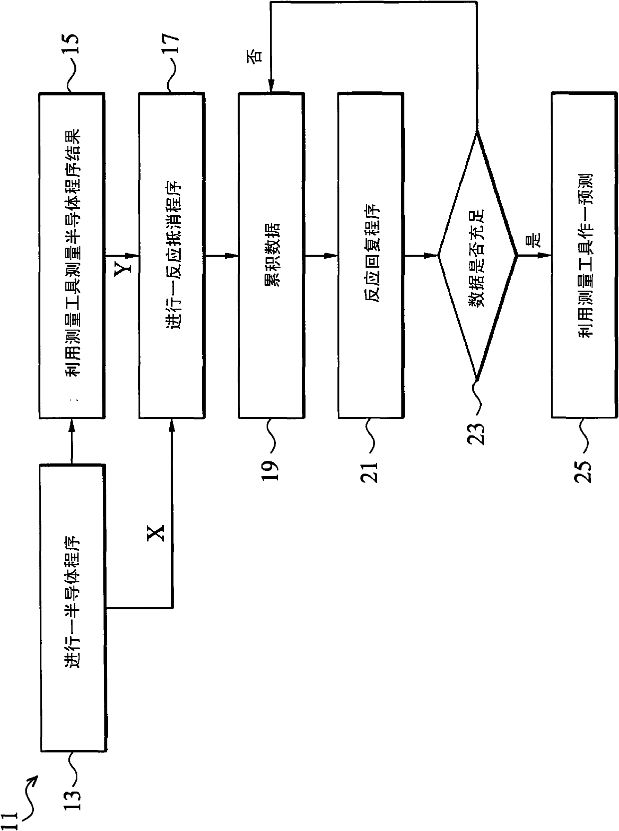
[0035] figure 1 A flowchart showing a method 11 of utilizing virtual metrology in semiconductor manufacturing according to an embodiment of the present invention. The above method begins the semiconductor manufacturing process at block 13 . The semiconductor fabrication process described above is associated with one or more fabrication tools, and the ...


PUM


Abstract

The present disclosure provides a method of fabricating a semiconductor device. The method includes collecting a plurality of manufacturing data sets from a plurality of semiconductor processes, respectively. The method includes normalizing each of the manufacturing data sets in a manner so that statistical differences among the manufacturing data sets are reduced. The method includes establishing a database that includes the normalized manufacturing data sets. The method includes normalizing the database in a manner so that the manufacturing data sets in the normalized database are statistically compatible with a selected one of the manufacturing data sets. The method includes predicting performance of a selected one of the semiconductor processes by using the normalized database. The selected semiconductor process corresponds to the selected manufacturing data set. The method includes controlling a semiconductor processing machine in response to the predicted performance.

Description

technical field [0001] The disclosure in this specification mainly relates to a measurement model, in particular to a virtual measurement system and method applied to semiconductor technology. Background technique [0002] Semiconductor integrated circuits are produced in a wafer fabrication plant (fab) through multiple processes. These procedures and related manufacturing tools can include thermal oxidation, diffusion, ion implantation, rapid thermal manufacturing (RTP), chemical vapor deposition (CVD), physical vapor deposition (PVD), epitaxy (epitaxy), etching (etch), and photoetching (photolithography). During the aforementioned manufacturing stages, the quality assurance and yield of semiconductor wafers are monitored using virtual metrology tools. [0003] Virtual metrology is a technique for predicting semiconductor process results based on modeling and pre-collected data (or training data). As semiconductor manufacturing methods advance (e.g., from 90nm to 65nm to...

Claims


Application Information

Patent Timeline
Patent Type & Authority Applications(China)
IPC IPC(8): H01L21/66H01L21/00
CPCH01L22/20
Inventor 蔡柏沣曾衍迪王若飞牟忠一
Owner TAIWAN SEMICON MFG CO LTD
Why Eureka
Try Eureka