Light emitting diode (LED) and manufacturing method thereof

A technology of light-emitting diodes and manufacturing methods, which is applied to electrical components, circuits, semiconductor devices, etc., can solve the problems of low light-emitting efficiency of light-emitting diodes, and achieve the effects of improving external quantum efficiency, improving internal quantum efficiency, and improving light utilization

Inactive Publication Date: 2011-08-24
ENRAYTEK OPTOELECTRONICS
View PDF3 Cites 2 Cited by
  • Summary
  • Abstract
  • Description
  • Claims
  • Application Information

AI Technical Summary

Problems solved by technology

[0005] The invention provides a light-emitting diode and its manufacturing method to solve the problem of low light extraction efficiency of the existing light-emitting diodes

Method used


Image

  • Light emitting diode (LED) and manufacturing method thereof
  • Light emitting diode (LED) and manufacturing method thereof
  • Light emitting diode (LED) and manufacturing method thereof

Examples


Embodiment Construction

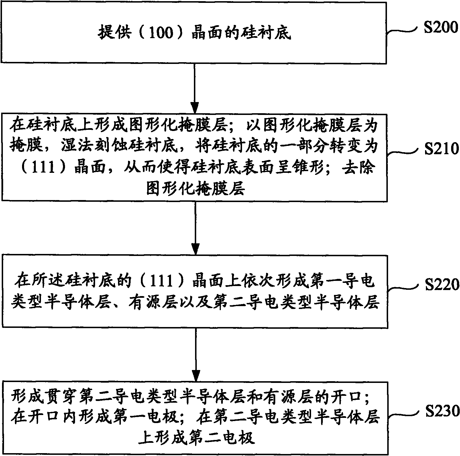
[0022] Please refer to figure 2 , which is a schematic flow chart of a method for manufacturing a light-emitting diode according to an embodiment of the present invention. In combination with this figure, the method includes the following steps:

[0023] Step S200, providing a silicon substrate with a (100) crystal plane;

[0024] Step S210, forming a patterned mask layer on the silicon substrate; using the patterned mask layer as a mask, wet etching the silicon substrate to transform a part of the silicon substrate into ( 111) a crystal plane, so that the surface of the silicon substrate is tapered; removing the patterned mask layer;

[0025] Step S220, sequentially forming a first conductivity type semiconductor layer, an active layer, and a second conductivity type semiconductor layer on the (111) crystal plane of the silicon substrate;

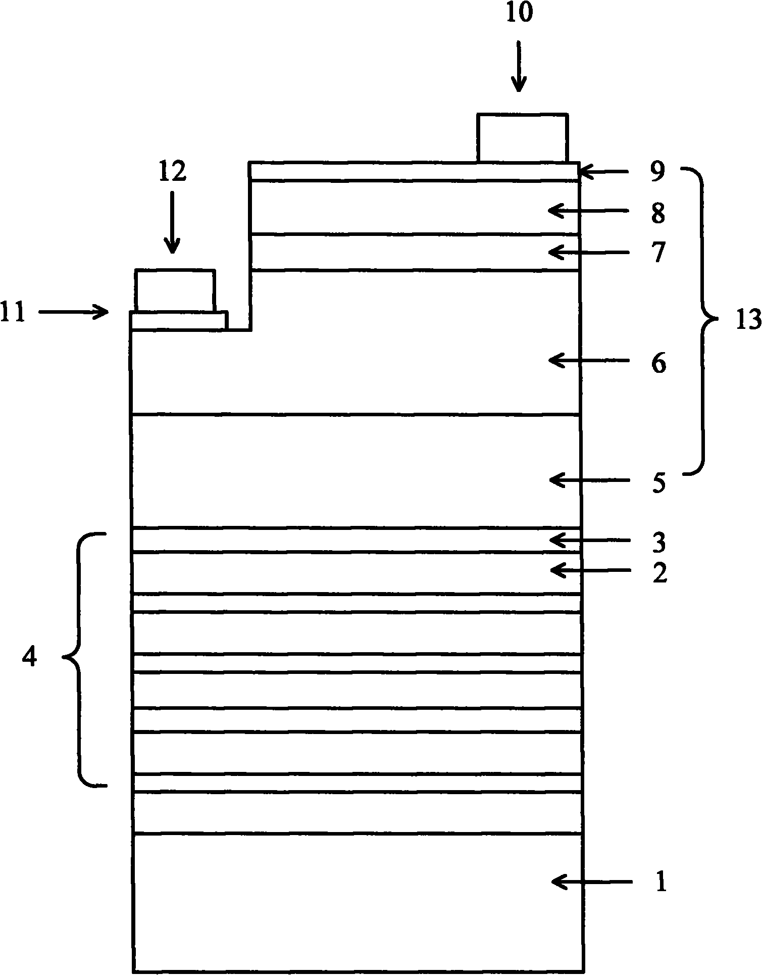
[0026] Step S230, forming an opening through the semiconductor layer of the second conductivity type and the active layer; forming a f...


PUM

PropertyMeasurementUnit
electrical resistivityaaaaaaaaaa

Abstract

The invention discloses a light emitting diode (LED) and a manufacturing method thereof. The method comprises the following steps of: providing a silicon substrate with a (100) crystal plane; taking a graphical mask layer as a mask, performing wet etching on the silicon substrate, and converting a part of the silicon substrate into a (111) crystal plane so as to make the surface of the silicon substrate conical; forming a first conductive semiconductor layer, an active layer and a second conductive semiconductor layer in turn on the (111) crystal plane of the silicon substrate; forming an opening which passes through the second conductive semiconductor layer and the active layer; forming a first electrode in the opening; and forming a second electrode on the second conductive semiconductor layer. The invention can improve the light utilization rate of the LED.

Description

technical field [0001] The invention relates to the field of semiconductor light emitting, in particular to a light emitting diode and a manufacturing method thereof. Background technique [0002] Light Emitting Diode (LED, Light Emitting Diode) is used in various fields due to its advantages of long life and low energy consumption, especially as its lighting performance index is greatly improved day by day, LED is often used as a light emitting device in the lighting field. Among them, gallium nitride (GaN) is the representative III-V compound semiconductor due to its wide band gap, high luminous efficiency, high electron saturation drift speed, and stable chemical properties. The field of optoelectronic devices has great application potential and has attracted widespread attention. [0003] However, the current semiconductor light-emitting diodes have the problem of low luminous efficiency. For ordinary unpackaged light-emitting diodes, the light extraction efficiency is...

Claims


Application Information

Patent Timeline
Patent Type & Authority Applications(China)
IPC IPC(8): H01L33/00H01L33/22H01L33/12H01L33/16H01L33/42
Inventor 肖德元张汝京程蒙召饶青
Owner ENRAYTEK OPTOELECTRONICS
Why Eureka
Try Eureka