
Multijunction solar cell with bonded transparent conductive interlayer

a solar cell and transparent technology, applied in the field of multijunction solar cells with transparent conductive interlayers, can solve the problems of lagging at least one of these three properties of bonded solar cell materials, limited materials that can be grown on a given substrate, etc., and achieve the effect of increasing efficiency

Active Publication Date: 2007-06-14
THE BOEING CO
View PDF6 Cites 81 Cited by
  • Summary
  • Abstract
  • Description
  • Claims
  • Application Information

AI Technical Summary

Benefits of technology

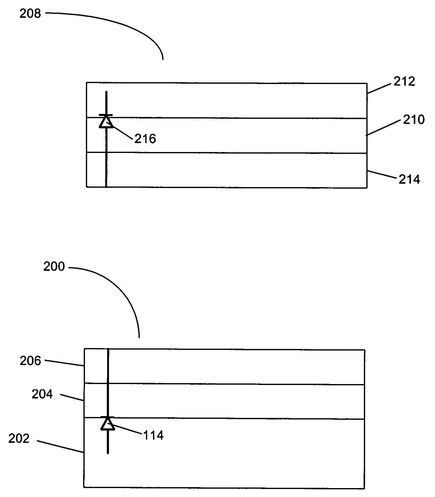
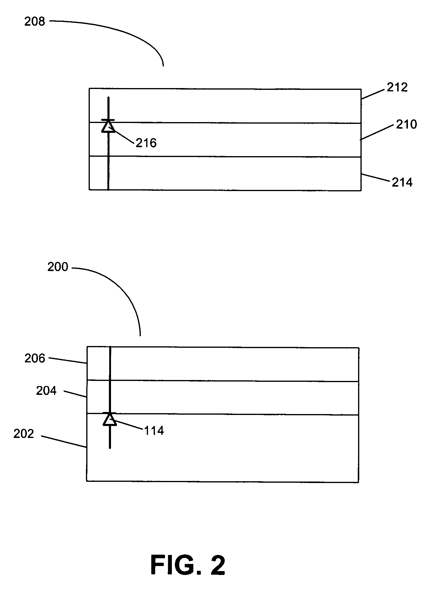
[0010] An apparatus in accordance with the present invention comprises two or more subcells bonded together using a Transparent Conductive Coating (TCC). TCC material is deposited on one or more surfaces to bond different subcells together. The TCC provides electrical contact between the two subcells while allowing for optical transmission. The thickness of the TCC may be used in conjunction with other optical coatings to optimize the transmission and reflection between the subcells to maximize the efficiency of the multijunction stack.
[0013] Such an apparatus further optionally comprises the second solar cell further comprising a second TCC layer, and the first solar cell is bonded to the second solar cell by bonding the first TCC layer to the second TCC layer, the second solar cell further comprising a second polarity electrode, a third solar cell, having a third TCC layer, wherein the third solar cell is bonded to the second solar cell by bonding the third TCC layer to the second solar cell, a dielectric stack, coupled to at least one TCC layer, a material for the first TCC layer being selected from a group comprising zinc oxide, indium zinc oxide, indium tin oxide, indium molybdenum oxide, indium titanium oxide, high-bandgap semiconductors such as GaInP, AlGaInP, AlGaAs, AlGaAsSb, AlInAs, AlGaInSb, AlGaInN, SiC, or ZnSeTe, a material for the second TCC layer being selected from a group comprising zinc oxide, indium zinc oxide, indium tin oxide, indium molybdenum oxide, indium titanium oxide, high-bandgap semiconductors such as GaInP, AlGaInP, AlGaAs, AlGaAsSb, AlInAs, AlGaInSb, AlGaInN, SiC, and ZnSeTe, an optical stack being used between the first cell and the second cell to reflect a range of wavelengths of light back through the second cell, one or more layers made of a transparent conductive material is incorporated into the optical stack, with at least one of a thickness, a position in the optical stack, composition, and an index of refraction of the one or more layers are designed to optimize reflection of a range of wavelengths back through the second cell, an optical stack is used between the first cell and the second cell to maximize light transmission for a range of wavelengths between the second cell and the first cell, and the first solar cell being a multijunction solar cell.
[0018] The present invention provides a solar cell that has increased efficiency. The present invention also provides a solar cell that can use a large range of materials to absorb different wavelengths of light. The present invention further provides a solar cell that can use these different materials while still keeping the materials bonded to each other.

Problems solved by technology

As such, the types of materials that can be grown on a given substrate are limited.
To date, bonded solar cell materials have lacked at least one of these three properties.

Method used


Image

  • Multijunction solar cell with bonded transparent conductive interlayer
  • Multijunction solar cell with bonded transparent conductive interlayer
  • Multijunction solar cell with bonded transparent conductive interlayer

Examples


Embodiment Construction

[0025] In the following description, reference is made to the accompanying drawings which form a part hereof, and which is shown, by way of illustration, several embodiments of the present invention. It is understood that other embodiments may be utilized and structural changes may be made without departing from the scope of the present invention.

Overview

[0026] The present invention utilizes transparent conductive materials, such as a Transparent Conductive Coating (TCC), in between the subcells of a multijunction solar cell to allow for a mismatch in the lattice constants of the subcell materials. Since the TCC is typically amorphous, the limitation on the lattice constants of the materials used in solar cell manufacture is removed, leaving designers to use materials based on efficiency and wavelength spectrum absorption. Further, use of TCC material frees the designer to choose different substrate materials if desired.

Standard Multijunction Solar Cell

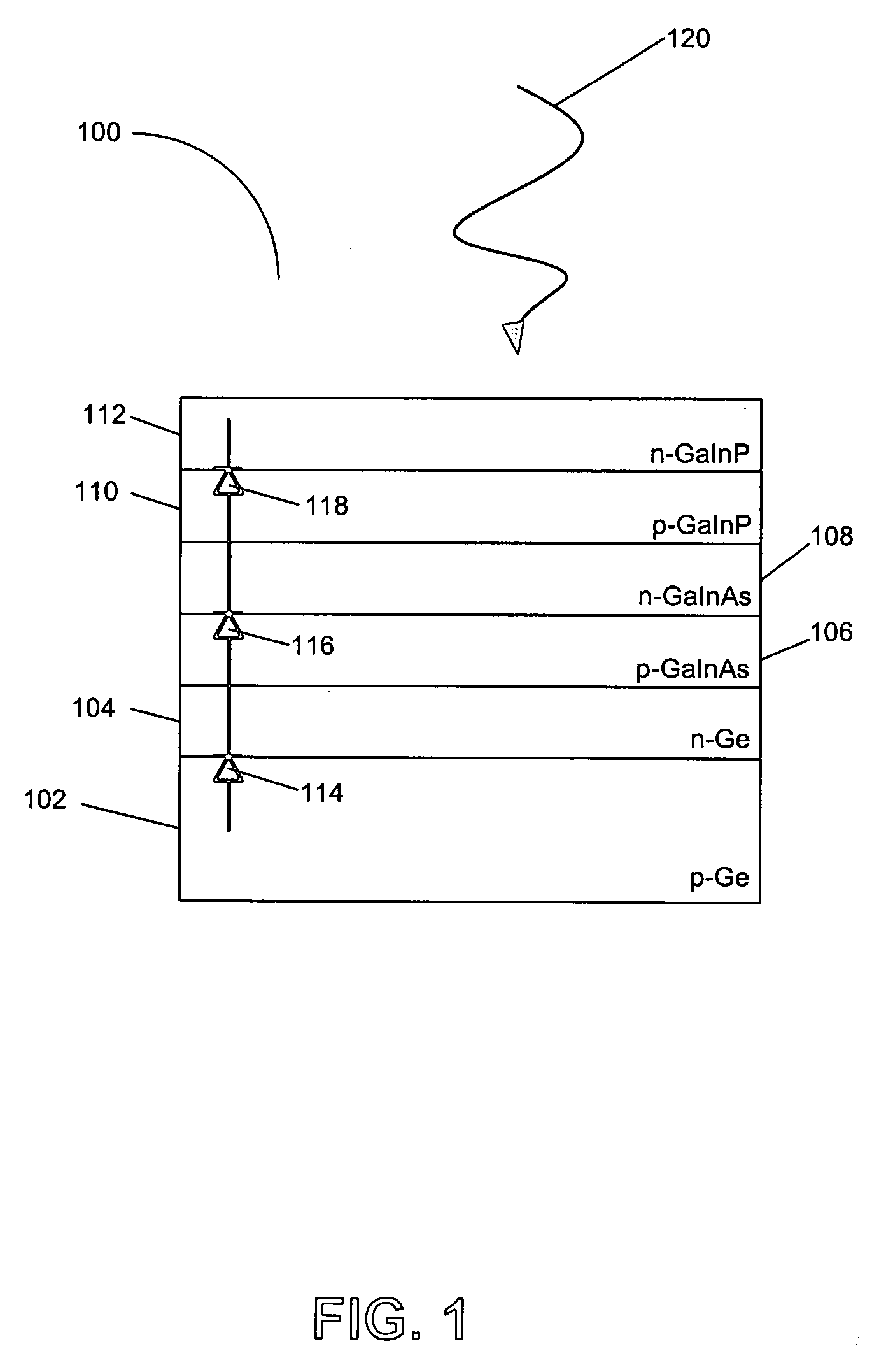
[0027]FIG. 1 illustrates...


PUM


Abstract

Methods and apparatuses for creating solar cell assemblies with bonded interlayers are disclosed. In summary, the present invention describes an apparatus and method for making a solar cell assembly with transparent conductive bonding interlayers. An apparatus in accordance with the present invention comprises a substrate, a first solar cell, coupled to a first side of the substrate, wherein the first solar cell comprises a first Transparent Conductive Coating (TCC) layer coupled to a first polarity electrode of the first solar cell, and a second solar cell, the second solar cell being bonded to the first solar cell by bonding the first TCC layer to the second solar cell.

Description

BACKGROUND OF THE INVENTION [0001] 1. Field of the Invention [0002] The present invention relates to devices and methods for making semiconductor devices, and in particular to a device and method for making a multijunction solar cell with a transparent conductive interlayer. [0003] 2. Description of the Related Art [0004] Solar cells are used in various technologies to provide power to other electronic assemblies. Satellites, calculators, and power systems are all examples of solar cell usage. [0005] A solar cell is a p-n junction created over a large area on a semiconductor substrate. The junction creates a voltage and current when light of certain wavelengths strike the surface of the solar cell, and, as such, solar cells are photovoltaic devices. These photovoltaic cells provide a lightweight, maintenance-free power source for various applications, and also provide a pollution-free, distributed energy generation source for use in power delivery systems. [0006] Typical high-effici...

Claims


Application Information

Patent Timeline
IPC IPC(8): H01L31/00
CPCH01L31/022466H01L31/0687H01L31/0725H01L31/076H01L31/1884Y02E10/544Y02E10/548Y02E10/547
Inventor KINSEY, GEOFFREY S.KING, RICHARD R.YOON, HOJUNMCALISTER, DENTON W.
Owner THE BOEING CO
Learn More